

Produsen Custom Global, Integrator, Consolidator, Mitra Outsourcing kanggo Macem-macem Produk & Layanan.
Kita minangka sumber siji-mandeg kanggo manufaktur, fabrikasi, teknik, konsolidasi, integrasi, outsourcing produk & layanan sing digawe khusus lan ora kasedhiya. Kita uga label pribadi / label putih produk sampeyan kanthi jeneng merek yen sampeyan pengin.
Pilih Basa sampeyan
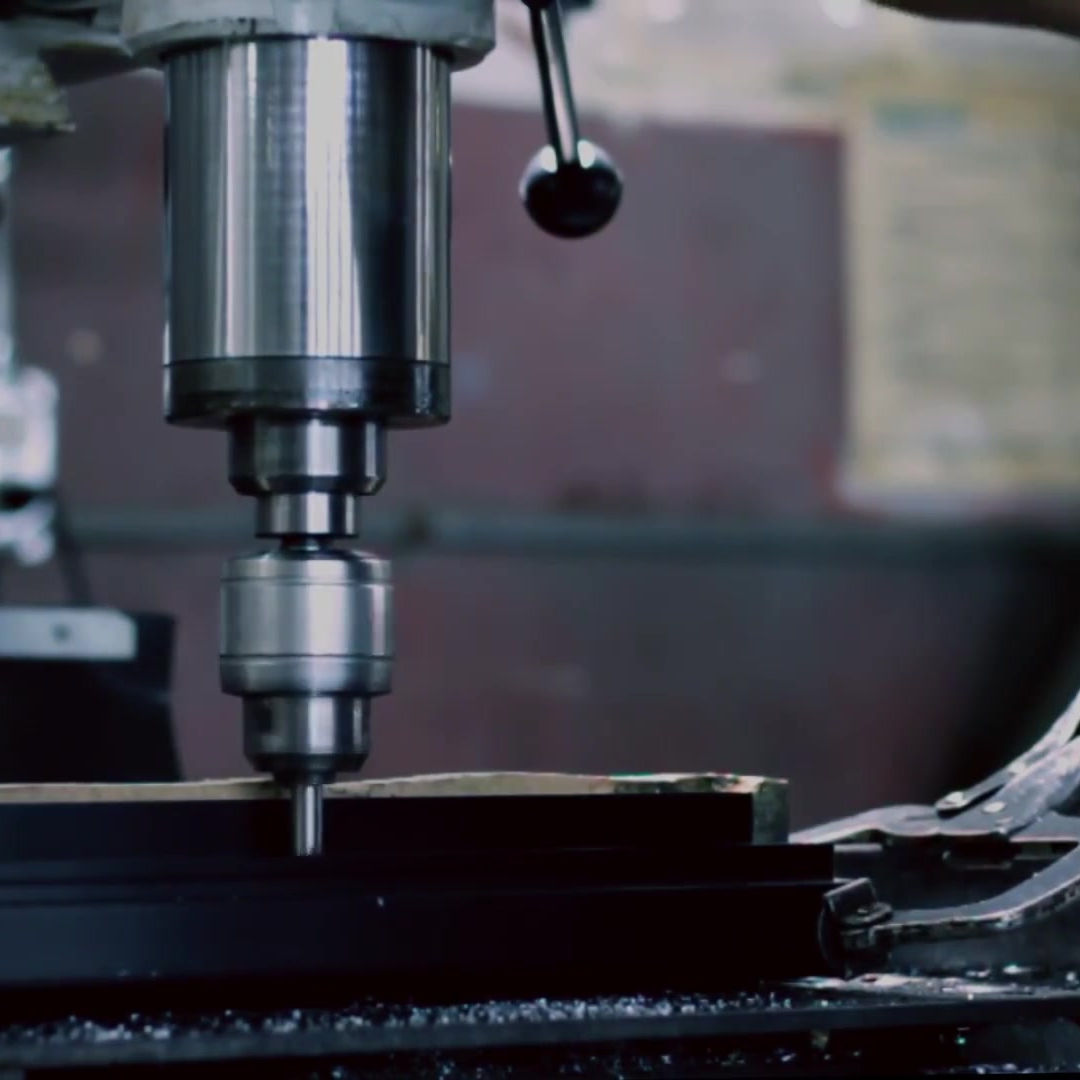
Manufaktur Custom Parts, Komponen, Rakitan, Produk Rampung, Mesin lan Peralatan Industri
Manufaktur Kontrak Domestik & Global
Outsourcing Produksi
Domestik, Pengadaan Global Produk Industri
Labeling pribadi / Label Putih Produk sampeyan nganggo Jeneng merek sampeyan
Product Finding & Locating Services
Desain Global lan Kemitraan Saluran
Integrasi Teknik
Layanan Teknik
Konsolidasi Global, Gudang, Logistik


Search Results
164 results found with an empty search
- Custom Made Products Data Entry
Custom Made Products Data Entry, Custom Manufactured Parts, Assemblies, Plastic Molds, Casting, CNC Machining, Extrusion, Metal Forging, Spring Manufacturing, Products Assembly, PCBA, PCB AGS-TECH, Inc. Panjenengan Produsen Kustom Global, Integrator, Konsolidator, Mitra Outsourcing. Kita minangka sumber siji-mandeg kanggo manufaktur, fabrikasi, teknik, konsolidasi, outsourcing. Isi info sampeyan yen sampeyan butuh desain & pangembangan khusus & prototipe & produksi massal: Yen ngisi formulir ing ngisor iki ora bisa utawa angel banget, kita uga nampa panjaluk sampeyan liwat email. Cukup nulis kita ing sales@agstech.net Get a Price Quote on a custom designed, developed, prototyped or manufactured product. First name Last name Email Phone Product Name Your Application for the Product Quantity Needed Do you have a price target ? If you do have, please let us know your expected price: Give us more details if you want: Do you accept offshore manufacturing ? YES NO Yen sampeyan duwe, upload file sing cocog karo produk kanthi ngeklik link ing ngisor iki. Aja kuwatir, link ing ngisor iki bakal mbukak jendhela anyar kanggo ndownload file sampeyan. Sampeyan ora bakal navigasi adoh saka jendhela saiki iki. Sawise ngunggah file, nutup MUNG Jendhela Dropbox, nanging ora kaca iki. Priksa manawa sampeyan ngisi kabeh spasi lan klik tombol kirim ing ngisor iki. File sing bakal mbantu kita ngutip produk khusus sampeyan yaiku gambar teknis, tagihan bahan, foto, sketsa....etc. Sampeyan bisa ngundhuh luwih saka siji file. KLIK kene kanggo upload file Request a Quote Thanks! We’ll send you a price quote shortly. PAGE sadurunge Kita AGS-TECH Inc., sumber siji-mandeg kanggo manufaktur & fabrikasi & engineering & outsourcing & konsolidasi. Kita minangka integrator teknik paling maneka warna ing Donya sing nawakake sampeyan manufaktur khusus, subassembly, perakitan produk lan layanan teknik.
- Mechanical Testing Instruments - Tension Tester - Torsion Test Machine
Mechanical Testing Instruments - Tension Tester - Torsion Test Machine - Bending Tester - Impact Test Device - Concrete Tester - Compression Testing Machine - H Instrumen Tes Mekanik Among the large number of MECHANICAL TEST INSTRUMENTS we focus our attention to the most essential and popular ones: IMPACT TESTERS, CONCRETE TESTERS / SCHMIDT HAMMER, TENSION TESTERS, COMPRESSION TESTING MACHINES, TORSION TEST EQUIPMENT, FATIGUE TEST MACHINE, THREE & FOUR POINT BENDING TESTERS, COEFFICIENT OF FRICTION TESTERS, HARDNESS & THICKNESS TESTERS, SURFACE ROUGHNESS TESTERS, VIBRATION METERS, TACHOMETERS, PRECISION ANALYTICAL BALANCE. We offer our customers quality brands such as ELCOMETER, SADT, SINOAGE for under list prices. Please choose from the downloadable catalogs below the brand name and model number of the equipment you need and tell us whether you want a brand new or refurbished / used equipment: AMETEK-LLOYD Instruments Materials Testing (Versatile Materials Testing Equipment, Universal Test Machines, Tensile Strength, Compressibility, Hardness, Elasticity, Peeling, Adhesion...etc.) ELCOMETER Inspection Equipment Catalog ( Physical Test Equipment , Concrete Inspection Equipment, Concrete Test Hammers, Fineness Of Grind/Dispersion , Density & Specific Gravity , Viscosity & Flow Measurement , Film Application & Test Charts , Drying Time & Permeability , Washability & Abrasion , Hardness & Scratch Resistance , Elasticity, Bend & Impact Testers , Flash Point ) HAIDA Adhesive Tape Peel Test Machine HAIDA Computerized Universal Test Machine with Extensometer HAIDA Computerized Universal Test Machine with Large Capacity (Double Column) HAIDA Computer Servo Tensile Test Machine HAIDA Desktop Tensile Test Machine HAIDA Double-Column Universal Testing Machine HAIDA Electro-Hydraulic Universal Testing Machine HAIDA Extra - Height Tensile Test Machine HAIDA Tensile Test Machines HAIDA Universal Testing Machine HAIDA Universal Test Machine HAIDA Universal Test Machine with Temperature Chamber INSTRON Compression and Tension Test Instruments SADT-SINOAGE Brand Metrology and Test Equipment, please CLICK HERE. Here you will find some of these testing equipment such as concrete testers and surface roughness tester. Let us examine these test devices in some detail: SCHMIDT HAMMER / CONCRETE TESTER : This test instrument, also sometimes called a SWISS HAMMER or a REBOUND HAMMER, is a device to measure the elastic properties or strength of concrete or rock, mainly surface hardness and penetration resistance. The hammer measures the rebound of a spring-loaded mass impacting against the surface of the sample. The test hammer will hit the concrete with a predetermined energy. The hammer’s rebound depends on the hardness of the concrete and is measured by the test equipment. Taking a conversion chart as a reference, the rebound value can be used to determine the compressive strength. The Schmidt hammer is an arbitrary scale ranging from 10 to 100. Schmidt hammers come with several different energy ranges. Their energy ranges are: (i) Type L-0.735 Nm impact energy, (ii) Type N-2.207 Nm impact energy; and (iii) Type M-29.43 Nm impact energy. Local variation in the sample. To minimize local variation in the samples it is recommended to take a selection of readings and take their average value. Prior to testing, the Schmidt hammer needs to be calibrated using a calibration test anvil supplied by the manufacturer. 12 readings should be taken, dropping the highest and lowest, and then taking the average of the ten remaining readings. This method is considered an indirect measurement of the strength of the material. It provides an indication based on surface properties for comparison between samples. This test method for testing concrete is governed by ASTM C805. On the other hand, the ASTM D5873 standard describes the procedure for testing of rock. Inside of our SADT brand catalog you will find the following products: DIGITAL CONCRETE TEST HAMMER SADT Models HT-225D/HT-75D/HT-20D - The SADT Model HT-225D is an integrated digital concrete test hammer combining data processor and test hammer into a single unit. It is widely used for non destructive quality testing of concrete and building materials. From its rebound value, the compressive strength of concrete can be calculated out automatically. All test data can be stored in memory and transferred to PC by USB cable or wirelessly by Bluetooth. The models HT-225D and HT-75D have measuring range of 10 – 70N/mm2, whereas the model HT-20D has only 1 – 25N/mm2. The impact energy of HT-225D is 0.225 Kgm and is suitable for testing ordinary building and bridge construction, the impact energy of HT-75D is 0.075 Kgm and is suitable for testing small and impact-sensitive parts of concrete and artificial brick, and finally the impact energy of HT-20D is 0.020Kgm and suitable for testing mortar or clay products. IMPACT TESTERS: In many manufacturing operations and during their service lives, many components need to be subjected to impact loading. In the impact test, the notched specimen is placed in an impact tester and broken with a swinging pendulum. There are two major types of this test: The CHARPY TEST and the IZOD TEST. For the Charpy test the specimen are supported at both ends, whereas for the Izod test they are supported only at one end like a cantilever beam. From the amount of swing of the pendulum, the energy dissipated in breaking the specimen is obtained, this energy is the impact toughness of the material. Using the impact tests, we can determine the ductile-brittle transition temperatures of materials. Materials with high impact resistance generally have high strength and ductility. These tests also reveal the sensitivity of a material’s impact toughness to surface defects, because the notch in the specimen can be considered a surface defect. TENSION TESTER : The strength-deformation characteristics of materials are determined using this test. Test specimen are prepared according to ASTM standards. Typically, solid and round specimens are tested, but flat sheets and tubular samples may also be tested using tension test. The original length of a specimen is the distance between gage marks on it and is typically 50 mm long. It is denoted as lo. Longer or shorter lengths can be used depending on the specimens and products. The original cross-sectional area is denoted as Ao. The engineering stress or also called nominal stress is then given as: Sigma = P / Ao And the engineering strain is given as: e = (l – lo) / lo In the linear elastic region, the specimen elongates proportionately to the load up to the proportional limit. Beyond this limit, even though not linearly, the specimen will continue to deform elastically up to the yield point Y. In this elastic region, the material will return to its original length if we remove the load. Hooke’s Law applies in this region and gives us the Young’s Modulus: E = Sigma / e If we increase the load and move beyond the yield point Y, the material begins to yield. In other words, the specimen begins to undergo plastic deformation. Plastic deformation means permanent deformation. The cross-sectional area of the specimen decreases permanently and uniformly. If specimen is unloaded at this point, the curve follows a straight line downward and parallel to the original line in the elastic region. If the load is further increased, the curve reaches a maximum and begins to decrease. The maximum stress point is called the tensile strength or ultimate tensile strength and is denoted as UTS. The UTS can be interpreted as the overall strength of materials. When load is greater than the UTS, necking occurs on the specimen and the elongation between gage marks is no longer uniform. In other words, the specimen becomes really thin at the location where necking occurs. During necking, the elastic stress drops. If the test is continued, the engineering stress drops further and the specimen fractures at the necking region. The stress level at fracture is the fracture stress. The strain at point of fracture is an indicator of ductility. The strain up to the UTS is referred to as uniform strain, and the elongation at fracture is referred to as total elongation. Elongation = ((lf – lo) / lo) x 100 Reduction of Area = ((Ao – Af) / Ao) x 100 Elongation and reduction of area are good indicators of ductility. COMPRESSION TESTING MACHINE ( COMPRESSION TESTER ) : In this test, the specimen is subjected to a compressive load contrary to the tensile test where the load is tensile. Generally, a solid cylindrical specimen is placed between two flat plates and compressed. Using lubricants at the contact surfaces, a phenomenon known as barreling is prevented. Engineering strain rate in compression is given by: de / dt = - v / ho, where v is die speed, ho original specimen height. True strain rate on the other hand is: de = dt = - v/ h, with h being the instantaneous specimen height. To keep the true strain rate constant during the test, a cam plastometer thru a cam action reduces the magnitude of v proportionally as the specimen height h decreases during the test. Using the compression test ductilities of materials are determined by observing cracks formed on barreled cylindrical surfaces. Another test with some differences in the die and workpiece geometries is the PLANE-STRAIN COMPRESSION TEST, which gives us the yield stress of the material in plane strain denoted widely as Y’. Yield stress of materials in plane strain can be estimated as: Y’ = 1.15 Y TORSION TEST MACHINES (TORSIONAL TESTERS) : The TORSION TEST is another widely used method for determining material properties. A tubular specimen with a reduced mid-section is used in this test. Shear stress, T is given by: T = T / 2 (Pi) (square of r) t Here, T is the applied torque, r is the mean radius and t is the thickness of the reduced section in the middle of the tube. Shear strain on the other hand is given by: ß = r Ø / l Here l is the length of the reduced section and Ø is the twist angle in radians. Within the elastic range, the shear modulus (modulus of rigidity) is expressed as: G = T / ß The relation between shear modulus and the modulus of elasticity is: G = E / 2( 1 + V ) The torsion test is applied to solid round bars at elevated temperatures to estimate the forgeability of metals. The more twists the material can withstand prior to failure, the more forgeable it is. THREE & FOUR POINT BENDING TESTERS : For brittle materials, the BEND TEST (also called FLEXURE TEST) is suitable. A rectangularly shaped specimen is supported at both ends and a load is applied vertically. The vertical force is applied at either one point as in the case of three point bending tester, or at two points as in the case of a four point test machine. The stress at fracture in bending is referred to as the modulus of rupture or transverse rupture strength. It is given as: Sigma = M c / I Here, M is the bending moment, c is one-half of the specimen depth and I is the moment of inertia of the cross-section. The magnitude of stress is the same in both three and four-point bending when all other parameters are kept constant. The four-point test is likely to result in a lower modulus of rupture as compared to the three-point test. Another superiority of the four-point bending test over the three point bending test is that its results are more consistent with less statistical scattering of values. FATIGUE TEST MACHINE: In FATIGUE TESTING, a specimen is subjected repeatedly to various states of stress. The stresses are generally a combination of tension, compression and torsion. The test process can be resembled to bending a piece of wire alternately in one direction, then the other until it fractures. The stress amplitude can be varied and is denoted as “S”. The number of cycles to cause total failure of the specimen is recorded and is denoted as “N”. Stress amplitude is the maximum stress value in tension and compression to which the specimen is subjected. One variation of the fatigue test is performed on a rotating shaft with a constant downward load. The endurance limit (fatigue limit) is defined as the max. stress value the material can withstand without fatigue failure regardless of the number of cycles. Fatigue strength of metals is related to their ultimate tensile strength UTS. COEFFICIENT OF FRICTION TESTER : This test equipment measures the ease with which two surfaces in contact are able to slide past one another. There are two different values associated with the coefficient of friction, namely the static and kinetic coefficient of friction. Static friction applies to the force necessary to initialize motion between the two surfaces and kinetic friction is the resistance to sliding once the surfaces are in relative motion. Appropriate measures need to be taken prior to testing and during testing to ensure freedom from dirt, grease and other contaminants that could adversely affect test results. ASTM D1894 is the main coefficient of friction test standard and is used by many industries with different applications and products. We are here to offer you the most suitable test equipment. If you need a custom set-up specifically designed for your application, we can modify existing equipment accordingly in order to meet your requirements and needs. HARDNESS TESTERS : Please go to our related page by clicking here THICKNESS TESTERS : Please go to our related page by clicking here SURFACE ROUGHNESS TESTERS : Please go to our related page by clicking here VIBRATION METERS : Please go to our related page by clicking here TACHOMETERS : Please go to our related page by clicking here For details and other similar equipment, please visit our equipment website: http://www.sourceindustrialsupply.com KLIK Product Finder-Locator Service PAGE sadurunge
- Microelectronics Manufacturing, Semiconductor Fabrication, Foundry, IC
Microelectronics Manufacturing, Semiconductor Fabrication - Foundry - FPGA - IC Assembly Packaging - AGS-TECH Inc. Mikroelektronika & Semikonduktor Manufaktur lan Fabrikasi Many of our nanomanufacturing, micromanufacturing and mesomanufacturing techniques and processes explained under the other menus can be used for MICROELECTRONICS MANUFACTURING too. However due to the importance of microelectronics in our products, we will concentrate on the subject specific applications of these processes here. Microelectronics related processes are also widely referred to as SEMICONDUCTOR FABRICATION processes. Our semiconductor engineering design and fabrication services include: - FPGA board design, development and programming - Microelectronics foundry services: Design, prototyping and manufacturing, third-party services - Semiconductor wafer preparation: Dicing, backgrinding, thinning, reticle placement, die sorting, pick and place, inspection - Microelectronic package design and fabrication: Both off-shelf and custom design and fabrication - Semiconductor IC assembly & packaging & test: Die, wire and chip bonding, encapsulation, assembly, marking and branding - Lead frames for semiconductor devices: Both off-shelf and custom design and fabrication - Design and fabrication of heat sinks for microelectronics: Both off-shelf and custom design and fabrication - Sensor & actuator design and fabrication: Both off-shelf and custom design and fabrication - Optoelectronic & photonic circuits design and fabrication Let us examine the microelectronics and semiconductor fabrication and test technologies in more detail so you can better understand the services and products we are offering. FPGA Board Design & Development and Programming: Field-programmable gate arrays (FPGAs) are reprogrammable silicon chips. Contrary to processors that you find in personal computers, programming an FPGA rewires the chip itself to implement user’s functionality rather than running a software application. Using prebuilt logic blocks and programmable routing resources, FPGA chips can be configured to implement custom hardware functionality without using a breadboard and soldering iron. Digital computing tasks are carried out in software and compiled down to a configuration file or bitstream that contains information on how the components should be wired together. FPGAs can be used to implement any logical function that an ASIC could perform and are completely reconfigurable and can be given a completely different “personality” by recompiling a different circuit configuration. FPGAs combine the best parts of application-specific integrated circuits (ASICs) and processor-based systems. These benefits include the following: • Faster I/O response times and specialized functionality • Exceeding the computing power of digital signal processors (DSPs) • Rapid prototyping and verification without the fabrication process of custom ASIC • Implementation of custom functionality with the reliability of dedicated deterministic hardware • Field-upgradable eliminating the expense of custom ASIC re-design and maintenance FPGAs provide speed and reliability, without requiring high volumes to justify the large upfront expense of custom ASIC design. Reprogrammable silicon also has the same flexibility of software running on processor-based systems, and it is not limited by the number of processing cores available. Unlike processors, FPGAs are truly parallel in nature, so different processing operations do not have to compete for the same resources. Each independent processing task is assigned to a dedicated section of the chip, and can function autonomously without any influence from other logic blocks. As a result, the performance of one part of the application is not affected when more processing is added on. Some FPGAs have analog features in addition to digital functions. Some common analog features are programmable slew rate and drive strength on each output pin, allowing the engineer to set slow rates on lightly loaded pins that would otherwise ring or couple unacceptably, and to set stronger, faster rates on heavily loaded pins on high-speed channels that would otherwise run too slowly. Another relatively common analog feature is differential comparators on input pins designed to be connected to differential signaling channels. Some mixed signal FPGAs have integrated peripheral analog-to-digital converters (ADCs) and digital-to-analog converters (DACs) with analog signal conditioning blocks that allow them to operate as a system-on-a-chip. Briefly, the top 5 benefits of FPGA chips are: 1. Good Performance 2. Short Time to Market 3. Low Cost 4. High Reliability 5. Long-Term Maintenance Capability Good Performance – With their capability of accommodating parallel processing, FPGAs have better computing power than digital signal processors (DSPs) and do not require sequential execution as DSPs and can accomplish more per clock cycles. Controlling inputs and outputs (I/O) at the hardware level provides faster response times and specialized functionality to closely match application requirements. Short Time to market - FPGAs offer flexibility and rapid prototyping capabilities and thus shorter time-to-market. Our customers can test an idea or concept and verify it in hardware without going through the long and expensive fabrication process of custom ASIC design. We can implement incremental changes and iterate on an FPGA design within hours instead of weeks. Commercial off-the-shelf hardware is also available with different types of I/O already connected to a user-programmable FPGA chip. The growing availability of high-level software tools offer valuable IP cores (prebuilt functions) for advanced control and signal processing. Low Cost—The nonrecurring engineering (NRE) expenses of custom ASIC designs exceed that of FPGA-based hardware solutions. The large initial investment in ASICs can be justified for OEMs producing many chips per year, however many end users need custom hardware functionality for the many systems in development. Our programmable silicon FPGA offers you something with no fabrication costs or long lead times for assembly. System requirements frequently change over time, and the cost of making incremental changes to FPGA designs is negligible when compared to the large expense of respinning an ASIC. High Reliability - Software tools provide the programming environment and FPGA circuitry is a true implementation of program execution. Processor-based systems generally involve multiple layers of abstraction to help task scheduling and share resources among multiple processes. The driver layer controls hardware resources and the OS manages memory and processor bandwidth. For any given processor core, only one instruction can execute at a time, and processor-based systems are continually at risk of time-critical tasks preempting one another. FPGAs, do not use OSs, pose minimum reliability concerns with their true parallel execution and deterministic hardware dedicated to every task. Long-term Maintenance Capability - FPGA chips are field-upgradable and do not require the time and cost involved with redesigning ASIC. Digital communication protocols, for example, have specifications that can change over time, and ASIC-based interfaces may cause maintenance and forward-compatibility challenges. To the contrary, reconfigurable FPGA chips can keep up with potentially necessary future modifications. As products and systems mature, our customers can make functional enhancements without spending time redesigning hardware and modifying the board layouts. Microelectronics Foundry Services: Our microelectronics foundry services include design, prototyping and manufacturing, third-party services. We provide our customers with assistance throughout the entire product development cycle - from design support to prototyping and manufacturing support of semiconductor chips. Our objective in design support services is to enable a first-time right approach for digital, analog, and mixed-signal designs of semiconductor devices. For example, MEMS specific simulation tools are available. Fabs that can handle 6 and 8 inch wafers for integrated CMOS and MEMS are at your service. We offer our clients design support for all major electronic design automation (EDA) platforms, supplying correct models, process design kits (PDK), analog and digital libraries, and design for manufacturing (DFM) support. We offer two prototyping options for all technologies: the Multi Product Wafer (MPW) service, where several devices are processed in parallel on one wafer, and the Multi Level Mask (MLM) service with four mask levels drawn on the same reticle. These are more economical than the full mask set. The MLM service is highly flexible compared to the fixed dates of the MPW service. Companies may prefer outsourcing semiconductor products to a microelectronics foundry for a number of reasons including the need for a second source, using internal resources for other products and services, willingness to go fabless and decrease risk and burden of running a semiconductor fab…etc. AGS-TECH offers open-platform microelectronics fabrication processes that can be scaled down for small wafer runs as well as mass manufacturing. Under certain circumstances, your existing microelectronics or MEMS fabrication tools or complete tool sets can be transferred as consigned tools or sold tools from your fab into our fab site, or your existing microelectronics and MEMS products can be redesigned using open platform process technologies and ported to a process available at our fab. This is faster and more economical than a custom technology transfer. If desired however customer’s existing microelectronics / MEMS fabrication processes may be transferred. Semiconductor Wafer Preparation: If desired by customers after wafers are microfabricated, we carry out dicing, backgrinding, thinning, reticle placement, die sorting, pick and place, inspection operations on semiconductor wafers. Semiconductor wafer processing involves metrology in between the various processing steps. For example, thin film test methods based on ellipsometry or reflectometry, are used to tightly control the thickness of gate oxide, as well as the thickness, refractive index and extinction coefficient of photoresist and other coatings. We use semiconductor wafer test equipment to verify that the wafers haven't been damaged by previous processing steps up until testing. Once the front-end processes have been completed, the semiconductor microelectronic devices are subjected to a variety of electrical tests to determine if they function properly. We refer to the proportion of microelectronics devices on the wafer found to perform properly as the “yield”. Testing of microelectronics chips on the wafer are carried out with an electronic tester that presses tiny probes against the semiconductor chip. The automated machine marks each bad microelectronics chip with a drop of dye. Wafer test data is logged into a central computer database and semiconductor chips are sorted into virtual bins according to predetermined test limits. The resulting binning data can be graphed, or logged, on a wafer map to trace manufacturing defects and mark bad chips. This map can also be used during wafer assembly and packaging. In final testing, microelectronics chips are tested again after packaging, because bond wires may be missing, or analog performance may be altered by the package. After a semiconductor wafer is tested, it is typically reduced in thickness before the wafer is scored and then broken into individual dies. This process is called semiconductor wafer dicing. We use automated pick-and-place machines specially manufactured for microelectronics industry to sort out the good and bad semiconductor dies. Only the good, unmarked semiconductor chips are packaged. Next, in the microelectronics plastic or ceramic packaging process we mount the semiconductor die, connect the die pads to the pins on the package, and seal the die. Tiny gold wires are used to connect the pads to the pins using automated machines. Chip scale package (CSP) is another microelectronics packaging technology. A plastic dual in-line package (DIP), like most packages, is multiple times larger than the actual semiconductor die placed inside, whereas CSP chips are nearly the size of the microelectronics die; and a CSP can be constructed for each die before the semiconductor wafer is diced. The packaged microelectronics chips are re-tested to make sure that they are not damaged during packaging and that the die-to-pin interconnect process was completed correctly. Using lasers we then etch the chip names and numbers on the package. Microelectronic Package Design and Fabrication: We offer both off-shelf and custom design and fabrication of microelectronic packages. As part of this service, modeling and simulation of microelectronic packages is also carried out. Modeling and simulation ensures virtual Design of Experiments (DoE) to achieve the optimal solution, rather than testing packages on the field. This reduces the cost and production time, especially for new product development in microelectronics. This work also gives us the opportunity to explain our customers how the assembly, reliability and testing will impact their microelectronic products. The primary objective of microelectronic packaging is to design an electronic system that will satisfy the requirements for a particular application at a reasonable cost. Because of the many options available to interconnect and house a microelectronics system, the choice of a packaging technology for a given application needs expert evaluation. Selection criteria for microelectronics packages may include some of the following technology drivers: -Wireability -Yield -Cost -Heat dissipation properties -Electromagnetic shielding performance -Mechanical toughness -Reliability These design considerations for microelectronics packages affect speed, functionality, junction temperatures, volume, weight and more. The primary goal is to select the most cost-effective yet reliable interconnection technology. We use sophisticated analysis methods and software to design microelectronics packages. Microelectronics packaging deals with the design of methods for the fabrication of interconnected miniature electronic systems and the reliability of those systems. Specifically, microelectronics packaging involves routing of signals while maintaining signal integrity, distributing ground and power to semiconductor integrated circuits, dispersing dissipated heat while maintaining structural and material integrity, and protecting the circuit from environmental hazards. Generally, methods for packaging microelectronics ICs involve the use of a PWB with connectors that provide the real-world I/Os to an electronic circuit. Traditional microelectronics packaging approaches involve the use of single packages. The main advantage of a single-chip package is the ability to fully test the microelectronics IC before interconnecting it to the underlying substrate. Such packaged semiconductor devices are either through-hole mounted or surface mounted to the PWB. Surface-mounted microelectronics packages do not require via holes to go through the entire board. Instead, surface-mounted microelectronics components can be soldered to both sides of the PWB, enabling higher circuit density. This approach is called surface-mount technology (SMT). The addition of area-array–style packages such as ball-grid arrays (BGAs) and chip-scale packages (CSPs) is making SMT competitive with the highest-density semiconductor microelectronics packaging technologies. A newer packaging technology involves the attachment of more than one semiconductor device onto a high-density interconnection substrate, which is then mounted in a large package, providing both I/O pins and environmental protection. This multichip module (MCM) technology is further characterized by the substrate technologies used to interconnect the attached ICs. MCM-D represents deposited thin film metal and dielectric multilayers. MCM-D substrates have the highest wiring densities of all MCM technologies thanks to the sophisticated semiconductor processing technologies. MCM-C refers to multilayered “ceramic” substrates, fired from stacked alternating layers of screened metal inks and unfired ceramic sheets. Using MCM-C we obtain a moderately dense wiring capacity. MCM-L refers to multilayer substrates made from stacked, metallized PWB “laminates,” that are individually patterned and then laminated. It used to be a low-density interconnect technology, however now MCM-L is quickly approaching the density of MCM-C and MCM-D microelectronics packaging technologies. Direct chip attach (DCA) or chip-on-board (COB) microelectronics packaging technology involves mounting the microelectronics ICs directly to the PWB. A plastic encapsulant, which is “globbed” over the bare IC and then cured, provides environmental protection. Microelectronics ICs can be interconnected to the substrate using either flip-chip, or wire bonding methods. DCA technology is particularly economical for systems that are limited to 10 or fewer semiconductor ICs, since larger numbers of chips can affect system yield and DCA assemblies can be difficult to rework. An advantage common to both the DCA and MCM packaging options is the elimination of the semiconductor IC package interconnection level, which allows closer proximity (shorter signal transmission delays) and reduced lead inductance. The primary disadvantage with both methods is the difficulty in purchasing fully tested microelectronics ICs. Other disadvantages of DCA and MCM-L technologies include poor thermal management thanks to the low thermal conductivity of PWB laminates and a poor coefficient of thermal expansion match between the semiconductor die and the substrate. Solving the thermal expansion mismatch problem requires an interposer substrate such as molybdenum for wire bonded die and an underfill epoxy for flip-chip die. The multichip carrier module (MCCM) combines all the positive aspects of DCA with MCM technology. The MCCM is simply a small MCM on a thin metal carrier that can be bonded or mechanically attached to a PWB. The metal bottom acts as both a heat dissipater and a stress interposer for the MCM substrate. The MCCM has peripheral leads for wire bonding, soldering, or tab bonding to a PWB. Bare semiconductor ICs are protected using a glob-top material. When you contact us, we will discuss your application and requirements to choose the best microelectronics packaging option for you. Semiconductor IC Assembly & Packaging & Test: As part of our microelectronics fabrication services we offer die, wire and chip bonding, encapsulation, assembly, marking and branding, testing. For a semiconductor chip or integrated microelectronics circuit to function, it needs to be connected to the system that it will control or provide instructions to. Microelectronics IC assembly does provide the connections for power and information transfer between the chip and the system. This is accomplished by connecting the microelectronics chip to a package or directly connecting it to the PCB for these functions. Connections between the chip and the package or printed circuit board (PCB) are via wire bonding, thru-hole or flip chip assembly. We are an industry leader in finding microelectronics IC packaging solutions to meet the complex requirements of the wireless and internet markets. We offer thousands of different package formats and sizes, ranging from traditional leadframe microelectronics IC packages for thru-hole and surface mount, to the latest chip scale (CSP) and ball grid array (BGA) solutions required in high pin count and high density applications. A wide variety of packages are available from stock including CABGA (Chip Array BGA), CQFP, CTBGA (Chip Array Thin Core BGA), CVBGA (Very Thin Chip Array BGA), Flip Chip, LCC, LGA, MQFP, PBGA, PDIP, PLCC, PoP - Package on Package, PoP TMV - Through Mold Via, SOIC / SOJ, SSOP, TQFP, TSOP, WLP (Wafer Level Package)…..etc. Wire bonding using copper, silver or gold are among the popular in microelectronics. Copper (Cu) wire has been a method of connecting silicon semiconductor dies to the microelectronics package terminals. With recent increase in gold (Au) wire cost, copper (Cu) wire is an attractive way to manage overall package cost in microelectronics. It also resembles gold (Au) wire due to its similar electrical properties. Self inductance and self capacitance are almost the same for gold (Au) and copper (Cu) wire with copper (Cu) wire having lower resistivity. In microelectronics applications where resistance due to bond wire can negatively impact circuit performance, using copper (Cu) wire can offer improvement. Copper, Palladium Coated Copper (PCC) and Silver (Ag) alloy wires have emerged as alternatives to gold bond wires due to cost. Copper-based wires are inexpensive and have low electrical resistivity. However, the hardness of copper makes it difficult to use in many applications such as those with fragile bond pad structures. For these applications, Ag-Alloy offers properties similar to those of gold while its cost is similar to that of PCC. Ag-Alloy wire is softer than PCC resulting in lower Al-Splash and lower risk of bond pad damage. Ag-Alloy wire is the best low cost replacement for applications that need die-to-die bonding, waterfall bonding, ultra-fine bond pad pitch and small bond pad openings, ultra low loop height. We provide a complete range of semiconductor testing services including wafer testing, various types of final testing, system level testing, strip testing and complete end-of-line services. We test a variety of semiconductor device types across all of our package families including radio frequency, analog and mixed signal, digital, power management, memory and various combinations such as ASIC, multi chip modules, System-in-Package (SiP), and stacked 3D packaging, sensors and MEMS devices such as accelerometers and pressure sensors. Our test hardware and contacting equipment are suitable for custom package size SiP, dual-sided contacting solutions for Package on Package (PoP), TMV PoP, FusionQuad sockets, multiple-row MicroLeadFrame, Fine-Pitch Copper Pillar. Test equipment and test floors are integrated with CIM / CAM tools, yield analysis and performance monitoring to deliver very high efficiency yield the first time. We offer numerous adaptive microelectronics test processes for our customers and offer distributed test flows for SiP and other complex assembly flows. AGS-TECH provides a full range of test consultation, development and engineering services across your entire semiconductor and microelectronics product lifecycle. We understand the unique markets and testing requirements for SiP, automotive, networking, gaming, graphics, computing, RF / wireless. Semiconductor manufacturing processes require fast and precisely controlled marking solutions. Marking speeds over 1000 characters/second and material penetration depths less than 25 microns are common in semiconductor microelectronics industry using advanced lasers. We are capable of marking mold compounds, wafers, ceramics and more with minimal heat input and perfect repeatability. We use lasers with high accuracy to mark even the smallest parts without damage. Lead frames for Semiconductor Devices: Both off-shelf and custom design and fabrication are possible. Lead frames are utilized in the semiconductor device assembly processes, and are essentially thin layers of metal that connect the wiring from tiny electrical terminals on the semiconductor microelectronics surface to the large-scale circuitry on electrical devices and PCBs. Lead frames are used in almost all semiconductor microelectronics packages. Most microelectronics IC packages are made by placing the semiconductor silicon chip on a lead frame, then wire bonding the chip to the metal leads of that lead frame, and subsequently covering the microelectronics chip with plastic cover. This simple and relatively low cost microelectronics packaging is still the best solution for many applications. Lead frames are produced in long strips, which allows them to be quickly processed on automated assembly machines, and generally two manufacturing processes are used: photo etching of some sort and stamping. In microelectronics lead frame design often demand is for customized specifications and features, designs that enhance electrical and thermal properties, and specific cycle time requirements. We have in-depth experience of microelectronics lead frame manufacturing for an array of different customers using laser assisted photo etching and stamping. Design and fabrication of heat sinks for microelectronics: Both off-shelf and custom design and fabrication. With the increase in heat dissipation from microelectronics devices and the reduction in overall form factors, thermal management becomes a more a more important element of electronic product design. The consistency in performance and life expectancy of electronic equipment are inversely related to the component temperature of the equipment. The relationship between the reliability and the operating temperature of a typical silicon semiconductor device shows that a reduction in the temperature corresponds to an exponential increase in the reliability and life expectancy of the device. Therefore, long life and reliable performance of a semiconductor microelectronics component may be achieved by effectively controlling the device operating temperature within the limits set by the designers. Heat sinks are devices that enhance heat dissipation from a hot surface, usually the outer case of a heat generating component, to a cooler ambient such as air. For the following discussions, air is assumed to be the cooling fluid. In most situations, heat transfer across the interface between the solid surface and the coolant air is the least efficient within the system, and the solid-air interface represents the greatest barrier for heat dissipation. A heat sink lowers this barrier mainly by increasing the surface area that is in direct contact with the coolant. This allows more heat to be dissipated and/or lowers the semiconductor device operating temperature. The primary purpose of a heat sink is to maintain the microelectronics device temperature below the maximum allowable temperature specified by the semiconductor device manufacturer. We can classify heat sinks in terms of manufacturing methods and their shapes. The most common types of air-cooled heat sinks include: - Stampings: Copper or aluminum sheet metals are stamped into desired shapes. they are used in traditional air cooling of electronic components and offer an economical solution to low density thermal problems. They are suitable for high volume production. - Extrusion: These heat sinks allow the formation of elaborate two-dimensional shapes capable of dissipating large heat loads. They may be cut, machined, and options added. A cross-cutting will produce omnidirectional, rectangular pin fin heat sinks, and incorporating serrated fins improves the performance by approximately 10 to 20%, but with a slower extrusion rate. Extrusion limits, such as the fin height-to-gap fin thickness, usually dictate the flexibility in design options. Typical fin height-to-gap aspect ratio of up to 6 and a minimum fin thickness of 1.3mm, are attainable with standard extrusion techniques. A 10 to 1 aspect ratio and a fin thickness of 0.8″can be obtained with special die design features. However, as the aspect ratio increases, the extrusion tolerance is compromised. - Bonded/Fabricated Fins: Most air cooled heat sinks are convection limited, and the overall thermal performance of an air cooled heat sink can often be improved significantly if more surface area can be exposed to the air stream. These high performance heat sinks utilize thermally conductive aluminum-filled epoxy to bond planar fins onto a grooved extrusion base plate. This process allows for a much greater fin height-to-gap aspect ratio of 20 to 40, significantly increasing the cooling capacity without increasing the need for volume. - Castings: Sand, lost wax and die casting processes for aluminum or copper / bronze are available with or without vacuum assistance. We use this technology for fabrication of high density pin fin heat sinks which provide maximum performance when using impingement cooling. - Folded Fins: Corrugated sheet metal from aluminum or copper increases surface area and the volumetric performance. The heat sink is then attached to either a base plate or directly to the heating surface via epoxy or brazing. It is not suitable for high profile heat sinks on account of the availability and fin efficiency. Hence, it allows high performance heat sinks to be fabricated. In selecting an appropriate heat sink meeting the required thermal criteria for your microelectronics applications, we need to examine various parameters that affect not only the heat sink performance itself, but also the overall performance of the system. The choice of a particular type of heat sink in microelectronics depends largely to the thermal budget allowed for the heat sink and external conditions surrounding the heat sink. There is never a single value of thermal resistance assigned to a given heat sink, since the thermal resistance varies with external cooling conditions. Sensor & Actuator Design and Fabrication: Both off-shelf and custom design and fabrication are available. We offer solutions with ready-to-use processes for inertial sensors, pressure and relative pressure sensors and IR temperature sensor devices. By using our IP blocks for accelerometers, IR and pressure sensors or applying your design according to available specifications and design rules, we can have MEMS based sensor devices delivered to you within weeks. Besides MEMS, other types of sensor and actuator structures can be fabricated. Optoelectronic & photonic circuits design and fabrication: A photonic or optical integrated circuit (PIC) is a device that integrates multiple photonic functions. It can be resembled to electronic integrated circuits in microelectronics. The major difference between the two is that a photonic integrated circuit provides functionality for information signals imposed on optical wavelengths in the visible spectrum or near infrared 850 nm-1650 nm. Fabrication techniques are similar to those used in microelectronics integrated circuits where photolithography is used to pattern wafers for etching and material deposition. Unlike semiconductor microelectronics where the primary device is the transistor, there is no single dominant device in optoelectronics. Photonic chips include low loss interconnect waveguides, power splitters, optical amplifiers, optical modulators, filters, lasers and detectors. These devices require a variety of different materials and fabrication techniques and therefore it is difficult to realize all of them on a single chip. Our applications of photonic integrated circuits are mainly in the areas of fiber-optic communication, biomedical and photonic computing. Some example optoelectronic products we can design and fabricate for you are LEDs (Light Emitting Diodes), diode lasers, optoelectronic receivers, photodiodes, laser distance modules, customized laser modules and more. KLIK Product Finder-Locator Service PAGE sadurunge
- Waterjet Machining, WJ Cutting, Abrasive Water Jet, WJM, AWJM, AJM
Waterjet Machining - WJ Cutting - Abrasive Water Jet - Hydrodynamic Machining - WJM - AWJM - AJM - AGS-TECH Inc. - USA Waterjet Machining & Abrasive Waterjet & Abrasive-Jet Machining lan Cutting The principle of operation of WATER-JET, ABRASIVE WATER-JET and ABRASIVE-JET MACHINING & CUTTING is based on momentum change of the fast flowing stream that hits the workpiece. During this momentum change, a strong force acts and cuts the workpiece. These WATERJET CUTTING & MACHINING (WJM) techniques are based on water and highly refined abrasives, propelled at three times the speed of sound, to make incredibly accurate and precise cuts in virtually any material. For some materials like leather and plastics, an abrasive may be omitted and cutting can be done only with water. Waterjet machining can do things that other techniques cannot, from cutting intricate, very thin details in stone, glass and metals; to rapid hole drilling of titanium. Our waterjet cutting machines can handle large flat stock material with many feet of dimensions with no limit to the type of material. To make cuts and manufacture parts, we can scan images from files into the computer or a Computer Aided Drawing (CAD) of your project can be prepared by our engineers. We need to determine the type of material being cut, its thickness, and the desired cut quality. Intricate designs present no problem as the nozzle simply follows the rendered image pattern. Designs are limited only by your imagination. Contact us today with your project and let us give you our suggestions and quote. Let us examine these three types of processes in detail. WATER-JET MACHINING (WJM): The process may equally be called HYDRODYNAMIC MACHINING. The highly localized forces from the water-jet are used for cutting and deburring operations. In simpler words, the water jet acts like a saw that cuts a narrow and smooth groove in the material. Pressures levels in waterjet-machining are around 400 MPa which is pretty sufficient for efficient operation. If needed, pressures that are a few times this value can be generated. The diameters of jet nozzles are in the neighborhood of 0.05 to 1mm. We cut a variety of nonmetallic materials such as fabrics, plastics, rubber, leather, insulating materials, paper, composite materials using the waterjet cutters. Even complicated shapes such as automotive dashboard coverings made of vinyl and foam can be cut using multiple-axis, CNC controlled waterjet machining equipment. Waterjet machining is an efficient and clean process when compared to other cutting processes. Some of the major advantages of this technique are: -Cuts can be started at any location on the work piece without the need to predrill holes. -No significant heat is produced -The waterjet machining and cutting process is well suited for flexible materials because no deflection and bending of the workpiece takes place. -The burrs produced are minimal -Water-jet cutting and machining is an environmentally friendly and safe process that uses water. ABRASIVE WATER-JET MACHINING (AWJM): In this process, abrasive particles such as silicon carbide or aluminum oxide are contained in the water jet. This increases the material removal rate over that of purely water-jet machining. Metallic, nonmetallic, composite materials and others can be cut using AWJM. The technique is particularly useful for us in cutting heat-sensitive materials that we cannot cut using other techniques that produce heat. We can produce minimum holes of 3mm size and maximum depths of about 25 mm. Cutting speed can reach as high as several meters per minute depending on material being machined. For metals the cutting speed in AWJM is less as compared to plastics. Using our multiple-axis robotic control machines we can machine complex three-dimensional parts to finish dimensions without the need for a second process. To keep nozzle dimensions and diameter constant we use sapphire nozzles which is important in keeping accuracy and repeatability of the cutting operations. ABRASIVE-JET MACHINING (AJM) : In this process a high-velocity jet of dry air, nitrogen or carbondioxide containing abrasive particles hits and cuts the workpiece under controlled conditions. Abrasive-Jet Machining is used for cutting small holes, slots and intricate patterns in very hard and brittle metallic and nonmetallic materials, deburring and removing flash from parts, trimming and beveling, removing surface films such as oxides, cleaning of components with irregular surfaces. The gas pressures are around 850 kPa, and the abrasive-jet velocities around 300 m/s. Abrasive particles have diameters around 10 to 50 microns. The high speed abrasive particles round off sharp corners and holes made tend to be tapered. Therefore designers of parts that will be machined by abrasive-jet should take these into consideration and make sure the produced parts do not require such sharp corners and holes. The water-jet, abrasive water-jet and abrasive-jet machining processes can be used effectively for cutting and deburring operations. These techniques have an inherent flexibility thanks to the fact that they do not use hard tooling. KLIK Product Finder-Locator Service PAGE sadurunge
- Hardness Tester - Rockwell - Brinell - Vickers - Leeb - Microhardness
Hardness Tester - Rockwell - Brinell - Vickers - Leeb - Microhardness - Universal - AGS-TECH Inc. - New Mexico - USA Panguji kekerasan AGS-TECH Inc. stocks a comprehensive range of hardness testers including ROCKWELL, BRINELL, VICKERS, LEEB, KNOOP, MICROHARDNESS TESTERS, UNIVERSAL HARDNESS TESTER, PORTABLE HARDNESS TESTING INSTRUMENTS, optical systems and software for measurement, data acquisition and analysis, test blocks, indenters, anvils and related accessories. Some of the brand name hardness testers we sell are BUEHLER, ELCOMETER, MITECH, SADT, SINOAGE, SINOWON ..... You can purchase brand new, refurbished or used equipment from us. Simply choose the product from the following catalogs and provide us the brand name and model of your choice: BUEHLER Hardness Testing Catalog ELCOMETER Inspection Equipment Catalog (does offer Physical Test Equipment , Concrete Inspection Equipment, Concrete Test Hammers , Hardness & Scratch Resistance Testers ) MITECH MH600 P ortable Hardness Tester MITECH Hardness Testers P roduct Comparison Table MITUTOYO Hardness Testing Machines SADT-SINOAGE B rand M etrology and T est E quipment Catalog SINOWON Rockwell Hardness Tester SINOWON Portable Ultrasonic Hardness Tester One of the most common tests for assessing the mechanical properties of materials is the hardness test. Hardness of a material is its resistance to permanent indentation. One may also say hardness is a material’s resistance to scratching and to wear. There are several techniques to measure the hardness of materials using various geometries and materials. The measurement results are not absolute, they are more of a relative comparative indicator, because the results depend on the shape of the indenter and the applied load. Our portable hardness testers can generally run any hardness test listed above. They can be configured for particular geometric features and materials such as hole interiors, gear teeth…etc. Let us briefly go over the various hardness test methods. BRINELL TEST : In this test, a steel or tungsten carbide ball with 10 mm diameter is pressed against a surface with a load of 500, 1500 or 3000 Kg force. Brinell hardness number is the ratio of the load to the curved area of indentation. A Brinell test leaves behind different types of impressions on the surface depending on the tested material’s condition. For example, on annealed materials a rounded profile is left behind whereas on cold-worked materials we observe a sharp profile. Tungsten carbide indenter balls are recommended for Brinell hardness numbers higher than 500. For harder workpiece materials a 1500 Kg or 3000 Kg load is recommended so that the impressions left behind are sufficiently large for accurate measurement. Because of the fact that impressions made by the same indenter at different loads are not geometrically similar, the Brinell hardness number depends on the load used. Therefore one should always note the load employed on the test results. Brinell test is well suited for materials between low to medium hardness. ROCKWELL TEST : In this test the depth of penetration is measured. The indenter is pressed on the surface initially with a minor load and then a major load. The difference in the penetration debth is a measure of hardness. Several Rockwell hardness scales exist employing different loads, indenter materials and geometries. The Rockwell hardness number is read directly from a dial on the testing machine. For example, if the hardness number is 55 using the C scale, it is written as 55 HRC. VICKERS TEST : Sometimes also referred to as the DIAMOND PYRAMID HARDNESS TEST, it uses a pyramid-shaped diamond indenter with loads ranging from 1 to 120 Kg. The Vickers hardness number is given by HV=1.854P / square L. The L here is the diagonal length of the diamond pyramid. The Vickers test gives basically the same hardness number regardless of the load. The Vickers test is suitable for testing materials with a wide range of hardness including very hard materials. KNOOP TEST : In this test, we use a diamond indenter in the shape of an elongated pyramid and loads between 25g to 5 Kg. The Knoop hardness number is given as HK=14.2P / square L. Here the letter L is the length of the elongated diagonal. The size of indentations in Knoop tests is relatively small, in the range of 0.01 to 0.10 mm. Due to this small number surface preparation for the material is very important. Test results should cite the load applied because the hardness number obtained depends on the applied load. Because light loads are used, the Knoop test is considered a MICROHARDNESS TEST. The Knoop test is therefore suitable for very small, thin specimens, brittle materials such as gemstones, glass and carbides, and even for measuring the hardness of individual grains in a metal. LEEB HARDNESS TEST : It is based on rebound technique measuring the Leeb hardness. It is an easy and industrially popular method. This portable method is mostly used for testing sufficiently large workpieces above 1 kg. An impact body with a hard metal test tip is propelled by spring force against the workpiece surface. When the impact body hits the workpiece, surface deformation takes place which will result in loss of kinetic energy. Velocity measurements reveal this loss in kinetic energy. When the impact body passes coil at a precise distance from the surface, a signal voltage is induced during the impact and rebound phases of the test. These voltages are proportional to the velocity. Using electronic signal processing one gets the Leeb hardness value from display. Our PORTABLE HARDNESS TESTERS from SADT / HARTIP HARDNESS TESTER SADT HARTIP2000/HARTIP2000 D&DL : This is an innovative portable Leeb hardness tester with newly patented technology, which makes HARTIP 2000 a universal angle (UA) impact direction hardness tester. There is no need to set up impact direction when taking measurements at any angle. Therefore, HARTIP 2000 offers a linear accuracy compared to the angle compensating method. HARTIP 2000 is also a cost saving hardness tester and has many other features. The HARTIP2000 DL is equipped with SADT unique D and DL 2-in-1 probe. SADT HARTIP1800 Plus/1800 Plus D&DL : This device is an advanced state-of-the-art palm sized metal hardness tester with many new features. Using a patented technology, SADT HARTIP1800 Plus is a new generation product. It has a high accuracy of +/-2 HL (or 0.3% @HL800) with high contract OLED display and wide environmental temperature range (-40ºC~60ºC). Apart from huge memories in 400 blocks with 360k data, HARTIP1800 Plus can download measured data to PC and printout to mini-printer by USB port and wirelessly with internal blue-tooth module. The battery can be charged simply from USB port. It has a customer re-calibration and statics function. HARTIP 1800 plus D&DL is equipped with two-in-one probe. With unique two-in-one probe, HARTIP1800plus D&DL can convert between probe D and probe DL simply by changing impact body. It’s more economical than buying them individually. It has the same configuration with HARTIP1800 plus except two-in-one probe. SADT HARTIP1800 Basic/1800 Basic D&DL : This is a basic model for HARTIP1800plus. With most of core functions of HARTIP1800 plus and a lower price, HARTIP1800 Basic is a good choice for the customer with limited budget. HARTIP1800 Basic also can be equipped with our unique D/DL two-in-one impact device. SADT HARTIP 3000 : This is an advanced hand-held digital metal hardness tester with high accuracy, wide measurement range and ease of operation. It is suitable for testing the hardness of all metals especially on site for large structural and assembled components, which are widely used in the power, petrochemical, aerospace, automotive and machine building industries. SADT HARTIP1500/HARTIP1000 : This is an integrated handheld metal hardness tester that combines impact device (probe) and processor into one unit. The size is much smaller than the standard impact device, which allows HARTIP 1500/1000 to meet not only normal measurement conditions, but also can take measurements at narrow spaces. HARTIP 1500/1000 is suitable for testing the hardness of almost all ferrous and nonferrous materials. With its new technology, its accuracy is improved to a higher level than the standard type. HARTIP 1500/1000 is one of the most economic hardness testers in its class. BRINELL HARDNESS READING AUTOMATIC MEASURING SYSTEM / SADT HB SCALER : HB Scaler is an optical measuring system which can automatically measure the size of indentation from Brinell hardness tester and gives the Brinell hardness readings. All values and indentation images can be saved in PC. With the software, all values can be processed and printed out as a report. Our BENCH HARDNESS TESTER products from SADT are: SADT HR-150A ROCKWELL HARDNESS TESTER : The manually operated HR-150A Rockwell hardness tester is known for its perfection and ease of operation. This machine uses the standard preliminary test force of 10kgf and main loads of 60/100/150 kilograms while conforming to the international Rockwell standard. After each test, the HR-150A shows the Rockwell B or Rockwell C hardness value directly on the dial indicator. The preliminary test force has to be applied manually, followed by applying the main load by means of the lever at the right side of the hardness tester. After unloading, the dial indicates the requested hardness value directly with high accuracy and repeatability. SADT HR-150DT MOTORIZED ROCKWELL HARDNESS TESTER : This series of hardness testers are recognized for their accuracy and ease of operation, function entirely conforming to the international Rockwell standard. Depending on the combination of indenter type and applied total test force, a unique symbol is given to each Rockwell scale. HR-150DT and HRM-45DT feature both specific Rockwell scales of HRC and HRB on a dial. The appropriate force should be adjusted manually, using the dial on the right side of the machine. After application of the preliminary force, the HR150DT and HRM-45DT will proceed with a fullly automated testing: loading, waiting, unloading, and at the end will display the hardness. SADT HRS-150 DIGITAL ROCKWELL HARDNESS TESTER : The HRS-150 digital Rockwell hardness tester is designed for ease of use and safety of operation. It conforms with the international Rockwell standard. Depending on the combination of indenter type and applied total test force, a unique symbol is given to each Rockwell scale. The HRS-150 will automatically show your selection of a specific Rockwell scale on the LCD display, and will indicate which load is being used. The integrated autobrake mechanism allows the preliminary test force to be applied manually without the possibility of an error. After application of the preliminary force, the HRS-150 will proceed with a fully automatic test: loading, dwell time, unloading, and computation of the hardness value and its display. Connected to the included printer through an RS232 output, it’s possible to print out all results. Our BENCH TYPE SUPERFICIAL ROCKWELL HARDNESS TESTER products from SADT are: SADT HRM-45DT MOTORIZED SUPERFICIAL ROCKWELL HARDNESS TESTER : This series hardness testers are recognized for their accuracy and ease of operation, perform entirely conforming to the international Rockwell standard. Depending on the combination of indenter type and applied total test force, a unique symbol is given to each Rockwell scale. HR-150DT and HRM-45DT feature both of the specific Rockwell scales HRC and HRB on a dial. The appropriate force should be adjusted manually, using the dial on the right side of the machine. After application of the preliminary force, the HR150DT and HRM-45DT will proceed with a fullly automatic test process: loading, dwelling, unloading, and at the end will display the hardness. SADT HRMS-45 SUPERFICIAL ROCKWELL HARDNESS TESTER : HRMS-45 Digital Superficial Rockwell Hardness Tester is a novel product integrating advanced mechanical and electronic technologies. The dual display of LCD and LED digital diodes, make it an upgraded product version of the standard type superficial Rockwell tester. It measures the hardness of ferrous, nonferrous metals and hard materials, carburized and nitrided layers, and other chemically treated layers. It is also used for the measurement of hardness of thin pieces. SADT XHR-150 PLASTIC ROCKWELL HARDNESS TESTER : XHR-150 plastics Rockwell hardness tester adopts a motorized testing method, testing force can be loaded, kept at dwelling and unloaded automatically. Human error is minimized and easy to operate. It is used to measure hard plastics, hard rubbers, aluminum, tin, copper, soft steel, synthetic resins, tribologic materials, etc. Our BENCH TYPE VICKERS HARDNESS TESTER products from SADT are: SADT HVS-10/50 LOW LOAD VICKERS HARDNESS TESTER : This low load Vicker’s hardness tester with digital display is a new hi-tech product integrating mechanical and photoelectrical technologies. As a substitute for traditional small-load Vicker’s hardness testers, it features an easy operation and good reliability, which is specially designed for testing small, thin samples or parts after surface coating. Suitable for research institutes, industrial labs and QC departments, this is an ideal hardness testing instrument for research and measurement purposes. It offers integration of computer programming technology, high resolution optical measuring system and photoelectrical technique, soft key input, light source adjustment, selectable testing model, conversion tables, pressure-holding time, file number input and data saving functions. It has a big LCD screen to display the test model, test pressure, indention length, hardness values, pressure holding time and the numbers of tests. Offers also date recording, test results recording and data processing, printing output function, through an RS232 interface. SADT HV-10/50 LOW LOAD VICKERS HARDNESS TESTER : These low load Vickers hardness testers are new hi-tech products integrating mechanical and photoelectrical technologies. These testers are specially designed for testing small and thin samples and parts after surface coating. Suitable for research institutes, industrial labs and QC departments. Key features and functions are microcomputer control, adjustment of light source via soft keys, adjustment of pressure holding time and LED/LCD display, its unique measurement conversion device and unique micro eyepiece one-time measurement readout device that ensures easy use and high accuracy. SADT HV-30 VICKERS HARDNESS TESTER : The HV-30 model Vickers hardness tester is specially designed for testing small, thin samples and parts after surface coating. Suitable for research institutes, factory labs and QC departments, these are ideal hardness testing instruments for research and test purposes. Key features and functions are micro computer control, automatic loading and unloading mechanism, adjustment of lighting source via hardware, adjustment of pressure holding time (0~30s), unique measurement conversion device and unique micro eyepiece one-time measurement readout device, ensuring easy use and high accuracy. Our BENCH TYPE MICRO HARDNESS TESTER products from SADT are: SADT HV-1000 MICRO HARDNESS TESTER / HVS-1000 DIGITAL MICRO HARDNESS TESTER : This product is especially well suited for high precision hardness testing of small and thin samples such as sheet, foil, coatings, ceramic products and hardened layers. To ensure a satisfactory indentation, the HV1000 / HVS1000 features automatic loading and unloading operations, a very accurate loading mechanism and a robust lever system. The micro-computer controlled system ensures an absolutely precise hardness measurement with adjustable dwell time. SADT DHV-1000 MICRO HARDNESS TESTER / DHV-1000Z DIGITAL VICKERS HARDNESS TESTER : These micro Vickers hardness testers made with a unique and precise design are able to produce a clearer indentation and hence a more accurate measurement. By means of a 20 × lens and a 40 × lens the instrument has a wider measurement field and a broader application range. Equipped with a digital microscope, on its LCD screen it shows the measuring methods, the test force, the indentation length, the hardness value, the dwell time of the test force as well as the number of the measurements. In addition, it is equipped with an interface linked to a digital camera and a CCD video camera. This tester is widely used for measuring ferrous metals, non-ferrous metals, IC thin sections, coatings, glass, ceramics, precious stones, quench hardened layers and more. SADT DXHV-1000 DIGITAL MICRO HARDNESS TESTER : These micro Vickers hardness testers made with a unique and precise are able to produce a clearer indentation and hence more accurate measurements. By means of a 20 × lens and a 40 × lens the tester has a wider measurement field and a broader application range. With an automatically turning device ( the automatically turning turret ), the operation has become easier; and with a threaded interface, it can be linked to a digital camera and a CCD video camera. First the device lets the LCD touch screen to be used, thus allowing the operation to be more human controlled. The device has capabilities such as direct reading of the measurements, the easy change of the hardness scales, the saving of the data, the printing and the connection with the RS232 interface. This tester is widely used for measuring ferrous metals, non-ferrous metals, IC thin sections, coatings, glass, ceramics, precious stones; thin plastic sections, quench hardened layers and more. Our BENCH TYPE BRINELL HARDNESS TESTER / MULTI-PURPOSE HARDNESS TESTER products from SADT are: SADT HD9-45 SUPERFICIAL ROCKWELL & VICKERS OPTICAL HARDNESS TESTER : This device serves the purpose of measuring the hardness of ferrous, nonferrous metals, hard metals, carburized and nitrided layers and chemically treated layers and thin pieces. SADT HBRVU-187.5 BRINELL ROCKWELL & VICKERS OPTICAL HARDNESS TESTER : This instrument is used for determining the Brinell, Rockwell and Vickers hardness of ferrous, nonferrous metals, hard metals, carburized layers and chemically treated layers. It can be used in plants, scientific & research institutes, laboratories and colleges. SADT HBRV-187.5 BRINELL ROCKWELL & VICKERS HARDNESS TESTER (NOT OPTICAL) : This instrument is used for determining the Brinell, Rockwell and Vickers hardness of ferrous, non-ferrous metals, hard metals, carburized layers and chemically treated layers. It can be used in factories, scientific & research institutes, laboratories and colleges. It’s not an optical type hardness tester. SADT HBE-3000A BRINELL HARDNESS TESTER : This automatic Brinell hardness tester features a wide measurement range up to 3000 Kgf with a high accuracy conforming to DIN 51225/1 standard. During the automatic test cycle the applied force will be controlled by a closed loop system guaranteeing a constant force on the work piece, conforming to DIN 50351 standard. The HBE-3000A comes completely with a reading microscope with enlargement factor 20X and a micrometer resolution of 0.005 mm. SADT HBS-3000 DIGITAL BRINELL HARDNESS TESTER : This digital Brinell hardness tester is a new generation state-of-the-art device. It can be used to determine the Brinell hardness of ferrous and non-ferrous metals. The tester offers electronic auto loading, computer software programming, high power optical measurement, photosensor and other features. Each operational process and test result can be displayed on its large LCD screen. The test results can be printed. Device is suitable for manufacturing environments, colleges and scientific institutions. SADT MHB-3000 DIGITAL ELECTRONIC BRINELL HARDNESS TESTER : This instrument is an integrated product combining optical, mechanical and electronic techniques, adopting a precise mechanical structure and computer controlled closed-circuit system. The instrument loads and unloads the testing force with its motor. Using a 0.5% accuracy compression sensor to feedback the information and the CPU to control, the instrument compensates automatically for the varying testing forces. Equipped with a digital micro eyepiece on the instrument, the length of indentation can be measured directly. All testing data such as the test method, the test force value, the length of test indentation, the hardness value and the dwell time of testing force can be shown on the LCD screen. There is no need to input the value of the diagonal length for the indentation and no need to look up the hardness value from the hardness table. Therefore the read data is more accurate and operation of this instrument is easier. For details and other similar equipment, please visit our equipment website: http://www.sourceindustrialsupply.com CLICK Product Finder-Locator Service PAGE sadurunge
- Active Optical Components, Lasers, Photodetectors, LED Dies, Laser
Active Optical Components - Lasers - Photodetectors - LED Dies - Photomicrosensor - Fiber Optic - AGS-TECH Inc. - USA Komponen Optik Aktif Manufaktur & Majelis The ACTIVE OPTICAL COMPONENTS we manufacture and supply are: • Lasers and photodetectors, PSD (Position Sensitive Detectors), quadcells and other optical sensors and sensor systems with electrical connections. Our active optical components span a large spectrum of wavelength regions. Whether your application is high power lasers for industrial cutting, drilling, welding...etc, or medical lasers for surgery or diagnostics, or telecommunication lasers or detectors suitable for the ITU grid, we are your one-stop source. Below are downloadable brochures for some of our off-the-shelf active optical components and devices. If you cannot find what you are searching for, please contact us and we will have something to offer you. We do also custom manufacture active optical components and assemblies according to your application and requirements. • Among the many achievements of our optical engineers is the concept design, optical and opto-mechanical design of optical scan head for GS 600 LASER DRILLING SYSTEM with dual galvo scanners and self compensating alignment. Since its introduction, the GS600 family has become the system of choice for many leading high volume manufacturers around the World. Using optical design tools such as ZEMAX and CodeV, our optical engineers are ready to design your custom systems. If you only have SOLIDWORKS files for your design, don't worry, send them and we will work out and create the optical design files, optimize & simulate and have you approve the final design. Even a hand sketch, a mockup, a prototype or sample is sufficient in most cases for us to take care of your product development needs. Click on blue highlighted text to download brochures and catalogs of some off-the-shelf-ready active optical products: Active fiber optic products Comprehensive electric & electronic components catalog for off-shelf products Hikrobot Machine Vision Products Hikrobot Smart Machine Vision Products Hikrobot Machine Vision Standard Products Hikvision Logistic Vision Solutions LED dies and chips Photomicrosensors Photosensors Photosensors and Photomicrosensors Sockets and Accessories Private Label Medical Endoscopes and Visualization Systems (We can put your company name and logo on these) Sensors & Analytical Measurement Systems for Optical OEM Applications in Liquid Analysis (We private label these with your brand name and logo if you wish. We can customize sensors to your needs and applications, OEM option available) Dowload brochure for our DESIGN PARTNERSHIP PROGRAM R e ference Code: OICASANLY KLIK Product Finder-Locator Service PAGE sadurunge
- Electric Discharge Machining, EDM, Spark Machining, Die Sinking
Electric Discharge Machining - EDM - Spark Machining - Die Sinking - Wire Erosion - Custom Manufacturing - AGS-TECH Inc. Mesin EDM, Penggilingan lan Penggilingan Listrik-Discharge ELECTRICAL DISCHARGE MACHINING (EDM), also referred to as SPARK-EROSION or ELECTRODISCHARGE MACHINING, SPARK ERODING, DIE SINKING or WIRE EROSION, is a NON-CONVENTIONAL MANUFACTURING process where erosion of metals takes place and desired shape is obtained using electrical discharges in the form of sparks. We also offer some varieties of EDM, namely NO-WEAR EDM, WIRE EDM (WEDM), EDM GRINDING (EDG), DIE-SINKING EDM, ELECTRICAL-DISCHARGE MILLING, micro-EDM, m-EDM and ELECTROCHEMICAL-DISCHARGE GRINDING (ECDG). Our EDM systems consist of shaped tools/electrode and the workpiece connected to DC power supplies and inserted in a electrically nonconducting dielectric fluid. After 1940 electrical discharge machining has become one of the most important and popular production technologies in manufacturing industries. When the distance between the two electrodes is reduced, the intensity of the electric field in the volume between the electrodes becomes greater than the strength of the dielectric in some points, which breaks, eventually forming a bridge for current to flow between the two electrodes. An intense electrical arc is generated causing significant heating to melt a portion of the workpiece and some of the tooling material. As a result, material is removed from both the electrodes. At the same time, the dielectric fluid is heated rapidly, resulting in evaporation of the fluid in the arc gap. Once the current flow stops or it is stopped heat is removed from the gas bubble by the surrounding dielectric fluid and the bubble cavitates (collapses). The shock wave created by the bubble’s collapse and the flow of dielectric fluid flush debris from the workpiece surface and entrain any molten workpiece material into the dielectric fluid. The repetition rate for these discharges are between 50 to 500 kHz, voltages between 50 to 380 V and currents between 0.1 and 500 Amperes. New liquid dielectric such as mineral oils, kerosene or distilled & deionized water is usually conveyed into the inter-electrode volume carrying away the solid particles (in the form of debris) and the insulating proprieties of the dielectric is restored. After a current flow, the potential difference between the two electrodes is restored to what it was before the breakdown, so a new liquid dielectric breakdown can occur. Our modern electrical discharge machines (EDM) offer numerically controlled movements and are equipped with pumps and filtering systems for the dielectric fluids. Electrical discharge machining (EDM) is a machining method mainly used for hard metals or those that would be very difficult to machine with conventional techniques. EDM typically works with any materials that are electrical conductors, although methods for machining insulating ceramics with EDM have also been proposed. The melting point and latent heat of melting are properties that determine the volume of metal removed per discharge. The higher these values, the slower the material removal rate. Because the electrical discharge machining process does not involve any mechanical energy, the hardness, strength, and toughness of the workpiece do not affect the removal rate. Discharge frequency or energy per discharge, the voltage and current are varied to control material removal rates. Rate of material removal and surface roughness increase with increasing current density and decreasing spark frequency. We can cut intricate contours or cavities in pre-hardened steel using EDM without the need for heat treatment to soften and re-harden them. We can use this method with any metal or metal alloys like titanium, hastelloy, kovar, and inconel. Applications of the EDM process include shaping of polycrystalline diamond tools. EDM is considered a non-traditional or non-conventional machining method along with processes such as electrochemical machining (ECM), water jet cutting (WJ, AWJ), laser cutting. On the other hand the conventional machining methods include turning, milling, grinding, drilling and other process whose material removal mechanism is essentially based on mechanical forces. Electrodes for electrical-discharge machining (EDM) are made of graphite, brass, copper and copper-tungsten alloy. Electrode diameters down to 0.1mm are possible. Since tool wear is an undesired phenomenon adversely affecting dimensional accuracy in EDM, we take advantage of a process called NO-WEAR EDM, by reversing polarity and using copper tools to minimize tool wear. Ideally speaking, the electrical-discharge machining (EDM) can be considered a series of breakdown and restoration of the dielectric liquid between the electrodes. In reality however, the removal of the debris from the inter-electrode area is almost always partial. This causes the electrical proprieties of the dielectric in the inter-electrodes area to be different from their nominal values and vary with time. The inter-electrode distance, (spark-gap), is adjusted by the control algorithms of the specific machine used. The spark-gap in EDM can unfortunately sometimes be short-circuited by the debris. The control system of the electrode may fail to react quickly enough to prevent the two electrodes (tool and workpiece) from short circuiting. This unwanted short circuit contributes to material removal differently from the ideal case. We pay utmost importance to flushing action in order to restore the insulating properties of the dielectric so that the current always happens in the point of the inter-electrode area, thereby minimizing the possibility of unwanted change of shape (damage) of the tool-electrode and workpiece. To obtain a specific geometry, the EDM tool is guided along the desired path very close to the workpiece without touching it, We pay utmost attention to the performance of motion control in use. This way, a large number of current discharges / sparks take place, and each contributes to the removal of material from both tool and workpiece, where small craters are formed. The size of the craters is a function of the technological parameters set for the specific job at hand and dimensions may range from the nanoscale (such as in the case of micro-EDM operations) to some hundreds of micrometers in roughing conditions. These small craters on the tool cause gradual erosion of the electrode called “tool wear”. To counteract the detrimental effect of the wear on the geometry of the workpiece we continuously replace the tool-electrode during a machining operation. Sometimes we achieve this by using a continuously replaced wire as electrode ( this EDM process is also called WIRE EDM ). Sometimes we use the tool-electrode in such a way that only a small portion of it is actually engaged in the machining process and this portion is changed on a regular basis. This is, for instance, the case when using a rotating disk as a tool-electrode. This process is called EDM GRINDING. Yet another technique we deploy consists of using a set of electrodes with different sizes and shapes during the same EDM operation to compensate for wear. We call this multiple electrode technique, and is most commonly used when the tool electrode replicates in negative the desired shape and is advanced towards the blank along a single direction, usually the vertical direction (i.e. z-axis). This resembles the sink of the tool into the dielectric liquid in which the workpiece is immersed, and therefore it is referred to as DIE-SINKING EDM (sometimes called CONVENTIONAL EDM or RAM EDM). The machines for this operation are called SINKER EDM. The electrodes for this type of EDM have complex forms. If the final geometry is obtained using a usually simple-shaped electrode moved along several directions and is also subject to rotations, we call it EDM MILLING. The amount of wear is strictly dependent on the technological parameters used in the operation ( polarity, maximum current, open circuit voltage). For example, in micro-EDM, also known as m-EDM, these parameters are usually set at values which generates severe wear. Therefore, wear is a major problem in that area which we minimize using our accumulated know-how. For example to minimize wear to graphite electrodes, a digital generator, controllable within milliseconds, reverses polarity as electro-erosion takes place. This results in an effect similar to electroplating that continuously deposits the eroded graphite back on the electrode. In another method, a so-called ''Zero Wear'' circuit we minimize how often the discharge starts and stops, keeping it on for as long a time as possible. The material removal rate in electrical-discharge machining can be estimated from: MRR = 4 x 10 exp(4) x I x Tw exp (-1.23) Here MRR is in mm3/min, I is current in Amperes, Tw is workpiece melting point in K-273.15K. The exp stands for exponent. On the other hand, the wear rate Wt of the electrode can be obtained from: Wt = ( 1.1 x 10exp(11) ) x I x Ttexp(-2.38) Here Wt is in mm3/min and Tt is melting point of the electrode material in K-273.15K Finally, the wear ratio of the workpiece to electrode R can be obtained from: R = 2.25 x Trexp(-2.38) Here Tr is the ratio of melting points of workpiece to electrode. SINKER EDM : Sinker EDM, also referred to as CAVITY TYPE EDM or VOLUME EDM, consists of an electrode and workpiece submerged in an insulating liquid. The electrode and workpiece are connected to a power supply. The power supply generates an electrical potential between the two. As the electrode approaches the workpiece, dielectric breakdown occurs in the fluid, forming a plasma channel, and a small spark jumps. The sparks usually strike one at a time because it is highly unlikely that different locations in the inter-electrode space have identical local electrical characteristics which would enable a spark to occur in all such locations simultaneously. Hundreds of thousands of these sparks happen at random points between the electrode and the workpiece per second. As the base metal erodes, and the spark gap subsequently increases, the electrode is lowered automatically by our CNC machine so that the process can continue uninterrupted. Our equipment has controlling cycles known as ''on time'' and ''off time''. The on time setting determines the length or duration of the spark. A longer on time produces a deeper cavity for that spark and all subsequent sparks for that cycle, creating a rougher finish on the workpiece and vice versa. The off time is the period of time that one spark is replaced by another. A longer off time permits the dielectric fluid to flush through a nozzle to clean out the eroded debris, thereby avoiding a short circuit. These settings are adjusted in micro seconds. WIRE EDM : In WIRE ELECTRICAL DISCHARGE MACHINING (WEDM), also called WIRE-CUT EDM or WIRE CUTTING, we feed a thin single-strand metal wire of brass through the workpiece, which is submerged in a tank of dielectric fluid. Wire EDM is an important variation of EDM. We occasionally use wire-cut EDM to cut plates as thick as 300mm and to make punches, tools, and dies from hard metals that are difficult to machine with other manufacturing methods. In this process which resembles to contour cutting with a band saw, the wire, which is constantly fed from a spool, is held between upper and lower diamond guides. The CNC-controlled guides move in the x–y plane and the upper guide can also move independently in the z–u–v axis, giving rise to the ability to cut tapered and transitioning shapes (such as circle on the bottom and square at the top). The upper guide can control axis movements in x–y–u–v–i–j–k–l–. This allows the WEDM to cut very intricate and delicate shapes. The average cutting kerf of our equipment that achieves the best economic cost and machining time is 0.335 mm using Ø 0.25 brass, copper or tungsten wire. However the upper and lower diamond guides of our CNC equipment are accurate to about 0.004 mm, and can have a cutting path or kerf as small as 0.021 mm using Ø 0.02 mm wire. So really narrow cuts are possible. The cutting width is greater than the width of the wire because sparking occurs from the sides of the wire to the workpiece, causing erosion. This ''overcut'' is necessary, for many applications it is predictable and therefore can be compensated for ( in micro-EDM this is not often the case). The wire spools are long—an 8 kg spool of 0.25 mm wire is just over 19 kilometers in length. Wire diameter can be as small as 20 micrometres and the geometry precision is in the neighborhood of +/- 1 micrometer. We generally use the wire only once and recycle it because it is relatively inexpensive. It travels at a constant velocity of 0.15 to 9m/min and a constant kerf (slot) is maintained during a cut. In the wire-cut EDM process we use water as the dielectric fluid, controlling its resistivity and other electrical properties with filters and de-ionizer units. The water flushes the cut debris away from the cutting zone. Flushing is an important factor in determining the maximum feed rate for a given material thickness and therefore we keep it consistent. Cutting speed in wire EDM is stated in terms of the cross-sectional area cut per unit time, such as 18,000 mm2/hr for 50mm thick D2 tool steel. The linear cutting speed for this case would be 18,000/50 = 360mm/hr The material removal rate in wire EDM is: MRR = Vf x h x b Here MRR is in mm3/min, Vf is the feed rate of the wire into workpiece in mm/min, h is thickness or height in mm, and b is the kerf, which is: b = dw + 2s Here dw is wire diameter and s is gap between wire and workpiece in mm. Along with tighter tolerances, our modern multi axis EDM wire-cutting machining centers have added features such as multi heads for cutting two parts at the same time, controls for preventing wire breakage, automatic self-threading features in case of wire breakage, and programmed machining strategies to optimize the operation, straight and angular cutting capabilities. Wire-EDM offers us low residual stresses, because it does not require high cutting forces for removal of material. When the energy/power per pulse is relatively low (as in finishing operations), little change in the mechanical properties of a material is expected due to low residual stresses. ELECTRICAL-DISCHARGE GRINDING (EDG) : The grinding wheels do not contain abrasives, they are made of graphite or brass. Repetitive sparks between the rotating wheel and workpiece remove material from workpiece surfaces. The material removal rate is: MRR = K x I Here MRR is in mm3/min, I is current in Amperes, and K is workpiece material factor in mm3/A-min. We frequently use electrical-discharge grinding to saw narrow slits on components. We sometimes combine EDG (Electrical-Discharge Grinding) process with ECG (Electrochemical Grinding) process where material is removed by chemical action, the electrical discharges from the graphite wheel breaking up the oxide film and washed away by the electrolyte. The process is called ELECTROCHEMICAL-DISCHARGE GRINDING (ECDG). Even though the ECDG process consumes relatively more power, it is a faster process than the EDG. We mostly grind carbide tools using this technique. Applications of Electrical Discharge Machining: Prototype production: We use the EDM process in mold-making, tool and die manufacturing, as well as for making prototype and production parts, especially for the aerospace, automobile and electronics industries in which production quantities are relatively low. In Sinker EDM, a graphite, copper tungsten or pure copper electrode is machined into the desired (negative) shape and fed into the workpiece on the end of a vertical ram. Coinage die making: For the creation of dies for producing jewelry and badges by the coinage (stamping) process, the positive master may be made from sterling silver, since (with appropriate machine settings) the master is significantly eroded and is used only once. The resultant negative die is then hardened and used in a drop hammer to produce stamped flats from cutout sheet blanks of bronze, silver, or low proof gold alloy. For badges these flats may be further shaped to a curved surface by another die. This type of EDM is usually performed submerged in an oil-based dielectric. The finished object may be further refined by hard (glass) or soft (paint) enameling and/or electroplated with pure gold or nickel. Softer materials such as silver may be hand engraved as a refinement. Drilling of Small Holes: On our wire-cut EDM machines, we use small hole drilling EDM to make a through hole in a workpiece through which to thread the wire for the wire-cut EDM operation. Separate EDM heads specifically for small hole drilling are mounted on our wire-cut machines which allow large hardened plates to have finished parts eroded from them as needed and without pre-drilling. We also use small hole EDM to drill rows of holes into the edges of turbine blades used in jet engines. Gas flow through these small holes allows the engines to use higher temperatures than otherwise possible. The high-temperature, very hard, single crystal alloys these blades are made of makes conventional machining of these holes with high aspect ratio extremely difficult and even impossible. Other application areas for small hole EDM is to create microscopic orifices for fuel system components. Besides the integrated EDM heads, we deploy stand-alone small hole drilling EDM machines with x–y axes to machine blind or through holes. EDM drills bore holes with a long brass or copper tube electrode that rotates in a chuck with a constant flow of distilled or deionized water flowing through the electrode as a flushing agent and dielectric. Some small-hole drilling EDMs are able to drill through 100 mm of soft or even hardened steel in less than 10 seconds. Holes between 0.3 mm and 6.1 mm can be achieved in this drilling operation. Metal disintegration machining: We also have special EDM machines for the specific purpose of removing broken tools (drill bits or taps) from work pieces. This process is called ''metal disintegration machining''. Advantages and Disadvantages Electrical-Discharge Machining: Advantages of EDM include machining of: - Complex shapes that would otherwise be difficult to produce with conventional cutting tools - Extremely hard material to very close tolerances - Very small work pieces where conventional cutting tools may damage the part from excess cutting tool pressure. - There is no direct contact between tool and work piece. Therefore delicate sections and weak materials can be machined without any distortion. - A good surface finish can be obtained. - Very fine holes can be easily drilled. Disadvantages of EDM include: - The slow rate of material removal. - The additional time and cost used for creating electrodes for ram/sinker EDM. - Reproducing sharp corners on the workpiece is difficult due to electrode wear. - Power consumption is high. - ''Overcut'' is formed. - Excessive tool wear occurs during machining. - Electrically non-conductive materials can be machined only with specific set-up of the process. KLIK Product Finder-Locator Service PAGE sadurunge
- Custom Electric Electronics Manufacturing, Lighting, Display, PCB,PCBA
Custom Electric Electronics Manufacturing, Lighting, Display, Touchscreen, Cable Assembly, PCB, PCBA, Wireless Devices, Wire Harness, Microwave Components Pabrikan Produk Listrik & Elektronik Kustom Waca liyane Majelis & Interkoneksi Kabel Listrik & Elektronik Waca liyane PCB & PCBA Manufaktur lan Majelis Waca liyane Komponen Listrik & Energi lan Sistem Manufaktur lan Majelis Waca liyane Manufaktur & Majelis Piranti RF lan Nirkabel Waca liyane Komponen Microwave lan Sistem Manufaktur & Majelis Waca liyane Sistem Pencahayaan & Iluminasi Manufaktur lan Majelis Waca liyane Solenoida lan Komponen Elektromagnetik & Majelis Waca liyane Komponen lan Majelis Listrik & Elektronik Waca liyane Tampilan & Layar Demek & Monitor Pabrikan lan Perakitan Waca liyane Otomasi & Sistem Robotik Manufaktur lan Majelis Waca liyane Sistem Embedded & Komputer Industri & PC Panel Waca liyane Peralatan Uji Industri We offer: • Majelis Kabel Custom, PCB, Tampilan & Layar Demek (kayata iPod), Komponen Daya & Energi, Nirkabel, Microwave, Komponen Kontrol Gerakan, Produk Lampu, Komponen Elektromagnetik lan Elektronik. Kita mbangun produk miturut spesifikasi lan syarat tartamtu. Produk kita diprodhuksi ing ISO9001: 2000, QS9000, ISO14001, TS16949 lingkungan certified lan duwe CE, UL tandha lan ketemu standar industri kayata IEEE, ANSI. Sawise ditunjuk kanggo proyek sampeyan, kita bisa ngurus kabeh manufaktur, perakitan, uji coba, kualifikasi, pengiriman & bea cukai. Yen luwih seneng, kita bisa nyimpen bagean sampeyan, ngumpulake kit khusus, nyetak lan menehi label jeneng & merek perusahaan lan dikirim menyang pelanggan. Ing tembung liyane, kita bisa dadi gudang lan pusat distribusi yen sampeyan seneng iki. Amarga gudang kita ana ing cedhak pelabuhan laut utama, iki menehi keuntungan logistik. Contone, nalika produk sampeyan teka ing pelabuhan laut utama AS, kita bisa langsung ngeterake menyang gudang toko sing bisa disimpen, ngumpul, nggawe kit, relabel, nyithak, paket miturut pilihan sampeyan lan ngirim kapal menyang pelanggan yen sampeyan pengin. . Kita ora mung nyedhiyakake produk. Perusahaan kita nggarap kontrak khusus ing ngendi kita teka ing situs sampeyan, ngevaluasi proyek sampeyan ing situs lan ngembangake proposal proyek sing dirancang khusus kanggo sampeyan. Kita banjur ngirim tim sing berpengalaman kanggo ngleksanakake proyek kasebut. Conto kerja kontrak kalebu instalasi modul solar, generator angin, lampu LED lan sistem otomatisasi hemat energi ing fasilitas industri sampeyan kanggo nyuda tagihan energi, instalasi sistem deteksi serat optik kanggo ndeteksi kerusakan ing pipa sampeyan utawa kanggo ndeteksi kemungkinan penyusup sing mlebu ing omah sampeyan. papan. Kita njupuk proyek cilik uga proyek gedhe ing skala industri. Minangka langkah pisanan, kita bisa nyambungake sampeyan liwat telpon, telekonferensi utawa MSN messenger menyang anggota tim ahli, supaya sampeyan bisa komunikasi langsung menyang pakar, takon lan ngrembug proyek sampeyan. Yen perlu, kita bakal teka lan ngunjungi sampeyan. Yen sampeyan butuh produk kasebut utawa sampeyan duwe pitakon, hubungi +1-505-550-6501 utawa email ing sales@agstech.net Yen sampeyan seneng banget karo kemampuan teknik lan riset & pangembangan tinimbang kemampuan manufaktur, mula sampeyan ngajak sampeyan ngunjungi situs web teknik http://www.ags-engineering.com KLIK Product Finder-Locator Service PAGE sadurunge
- Keys Splines and Pins, Square Flat Key, Pratt and Whitney, Woodruff...
Keys Splines and Pins, Square Flat Key, Pratt and Whitney, Woodruff, Crowned Involute Ball Spline Manufacturing, Serrations, Gib-Head Key from AGS-TECH Inc. Keys & Splines & Pin Manufaktur Other miscellaneous fasteners we provide are keys, splines, pins, serrations. KEYS: A key is a piece of steel lying partly in a groove in the shaft and extending into another groove in the hub. A key is used to secure gears, pulleys, cranks, handles, and similar machine parts to shafts, so that the motion of the part is transmitted to the shaft, or the motion of the shaft to the part, without slippage. The key may also act in a safety capacity; its size can be calculated so that when overloading takes place, the key will shear or break before the part or shaft breaks or deforms. Our keys are also available with a taper on their top surfaces. For tapered keys, the keyway in the hub is tapered to accommodate the taper on the key. Some major types of keys we offer are: Square key Flat key Gib-Head Key – These keys are the same as flat or square tapered keys but with added head for ease of removal. Pratt and Whitney Key – These are rectangular keys with rounded edges. Two-thirds of these keys sit in the shaft and one-third in the hub. Woodruff Key – These keys are semicircular and fit into semicircular keyseats in the shafts and rectangular keyways in the hub. SPLINES: Splines are ridges or teeth on a drive shaft that mesh with grooves in a mating piece and transfer torque to it, maintaining the angular correspondence between them. Splines are capable of carrying heavier loads than keys, permit lateral movement of a part, parallel to the axis of the shaft, while maintaining positive rotation, and allow the attached part to be indexed or changed to another angular position. Some splines have straight-sided teeth, whereas others have curved-sided teeth. Splines with curved-sided teeth are called involute splines. Involute splines have pressure angles of 30, 37.5 or 45 degrees. Both internal and external spline versions are available. SERRATIONS are shallow involute splines with 45 degree pressure angles and are used for holding parts like plastic knobs. Major types of splines we offer are: Parallel key splines Straight-side splines – Also called parallel-side splines, they are used in many automotive and machine industry applications. Involute splines – These splines are similar in shape to involute gears but have pressure angles of 30, 37.5 or 45 degrees. Crowned splines Serrations Helical splines Ball splines PINS / PIN FASTENERS: Pin fasteners are an inexpensive and effective method of assembly when loading is primarily in shear. Pin fasteners can be separated into two groups: Semipermanent Pinsand Quick-Release Pins. Semipermanent pin fasteners require application of pressure or the aid of tools for installation or removal. Two basic types are Machine Pins and Radial Locking Pins. We offer the following machine pins: Hardened and ground dowel pins – We have standardized nominal diameters between 3 to 22 mm available and can machine custom sized dowel pins. Dowel pins can be used to hold laminated sections together, they can fasten machine parts with high alignment accuracy, lock components on shafts. Taper pins – Standard pins with 1:48 taper on the diameter. Taper pins are suitable for light-duty service of wheels and levers to shafts. Clevis pins - We have standardized nominal diameters between 5 to 25 mm available and can machine custom sized clevis pins. Clevis pins can be used on mating yokes, forks and eye members in knuckle joints. Cotter pins – Standardized nominal diameters of cotter pins range from 1 to 20 mm. Cotter pins are locking devices for other fasteners and are generally used with a castle or slotted nuts on bolts, screws, or studs. Cotter pins enable low-cost and convenient locknut assemblies. Two basic pin forms are offered as Radial Locking Pins, solid pins with grooved surfaces and hollow spring pins which are either slotted or come with spiral-wrapped configuration. We offer the following radial locking pins: Grooved straight pins – Locking is enabled by parallel, longitudinal grooves uniformly spaced around the pin surface. Hollow spring pins – These pins are compressed when driven into holes and pins exert spring pressure against the hole walls along their entire engaged length to produce locking fits Quick-release pins: Available types vary widely in head styles, types of locking and release mechanisms, and range of pin lengths. Quick-release pins have applications such as clevis-shackle pin, draw-bar hitch pin, rigid coupling pin, tubing lock pin, adjustment pin, swivel hinge pin. Our quick release pins can be grouped into one of two basic types: Push-pull pins – These pins are made with either a solid or hollow shank containing a detent assembly in the form of a locking lug, button or ball, backed up by some sort of plug, spring or resilient core. The detent member projects from the pins surface until sufficient force is applied in assembly or removal to overcome the spring action and to release the pins. Positive-locking pins - For some quick-release pins, the locking action is independent of insertion and removal forces. Positive-locking pins are suited for shear-load applications as well as for moderate tension loads. KLIK Product Finder-Locator Service PAGE sadurunge
- Industrial Leather Products, USA, AGS-TECH Inc.
Industrial leather products including honing and sharpening belts, leather transmission belts, sewing machine leather treadle belt, leather tool organizers and holders, leather gun holsters, leather steering wheel covers and more. Produk Kulit Industri Industrial leather products manufactured include: - Leather Honing and Sharpening Belts - Leather Transmission Belts - Sewing Machine Leather Treadle Belt - Leather Tool Organizers & Holders - Leather Gun Holsters Leather is a natural product with outstanding properties that make it a good fit for many applications. Industrial leather belts are used in power transmissions, as sewing machine leather treadle belts as well as fastening, securing, honing and sharpening of metal blades among many others. Besides our off-shelf industrial leather belts listed in our brochures, endless belts and special lengths / widths can also be produced for you. Applications of industrial leather includes Flat Leather Belting for power transmission and Round Leather Belting for Industrial Sewing Machines. Industrial leather is one of the oldest types of manufactured products. Our Vegetable Tanned Industrial leathers are pit tanned for many months and heavily dressed with a mixture of oils and greased to give its ultimate strength. Our Chrome Industrial Leathers can be manufactured in various ways, waxed, oiled or dry for moulding. We offer a chrome-retanned leather manufactured to withstand very high temperatures and they can be used for hydraulic applications and packings. Our Chrome Friction leathers are designed to have extraordinary abrasion properties. Various Shore Hardnesses are available. Many other applications of industrial leather products exist, including wearable tool organizers, tool holders, leather threads, steering wheel covers...etc. We are here to help you in your projects. A blueprint, a sketch, a photo or sample can serve to make us understand your product needs. We can either manufacture the industrial leather product according to your design, or we can help you in your design work and once you approve the final design, we can manufacture the product for you. Since we supply a wide variety of industrial leather products with different dimensions, applications and material grade; it is impossible to list them all here. We encourage you to email or call us so we can determine which product is the best fit for you. When contacting us, please make sure to inform us about: - Your application for the industrial leather products - Material grade desired & needed - Dimensions - Finish - Packaging requirements - Labeling requirements - Quantity PAGE sadurunge
- Micromanufacturing, Nanomanufacturing, Mesomanufacturing AGS-TECH Inc.
Micromanufacturing, Nanomanufacturing, Mesomanufacturing - Electronic & Magnetic Optical & Coatings, Thin Film, Nanotubes, MEMS, Microscale Fabrication Manufaktur Nanoscale & Microscale & Mesoscale Waca liyane Our NANOMANUFACTURING, MICROMANUFACTURING and MESOMANUFACTURING processes can be categorized as: Surface Treatments and Modification Functional Coatings / Decorative Coatings / Thin Film / Thick Film Nanoscale Manufacturing / Nanomanufacturing Microscale Manufacturing / Micromanufacturing / Micromachining Mesoscale Manufacturing / Mesomanufacturing Microelectronics & Semiconductor Manufacturing and Fabrication Microfluidic Devices Manufacturing Micro-Optics Manufacturing Micro Assembly and Packaging Soft Lithography In every smart product designed today, one can consider an element that will increase efficiency, versatility, reduce power consumption, reduce waste, increase lifetime of the product and thus be environmentally friendly. For this purpose, AGS-TECH is focusing on a number of processes and products that can be incorporated into devices and equipment to achieve these goals. For example low-friction FUNCTIONAL COATINGS can reduce power consumption. Some other functional coating examples are scratch resistant coatings, anti-wetting SURFACE TREATMENTS and coatings (hydrophobic), wetness promoting (hydrophilic) surface treatment and coatings, anti-fungal coatings, diamond like carbon coatings for cutting and scribing tools, THIN FILMelectronic coatings, thin film magnetic coatings, multilayer optical coatings. In NANOMANUFACTURING or NANOSCALE MANUFACTURING, we produce parts at nanometer length scales. In practice it refers to manufacturing operations below micrometer scale. Nanomanufacturing is still in its infancy when compared to micromanufacturing, however the trend is in that direction and nanomanufacturing is definitely very important for the near future. Some applications of nanomanufacturing today are carbon nanotubes as reinforcing fibers for composite materials in bicycle frames, baseball bats and tennis racquets. Carbon nanotubes, depending on the orientation of the graphite in the nanotube, can act as semiconductors or conductors. Carbon nanotubes have very high current-carrying capability, 1000 times higher than silver or copper. Another application of nanomanufacturing is nanophase ceramics. By using nanoparticles in producing ceramic materials, we can simultaneously increase both the strength and ductility of the ceramic. Please click on the submenu for more information. MICROSCALE MANUFACTURING or MICROMANUFACTURING refers to our manufacturing and fabrication processes on a microscopic scale not visible to the naked eye. The terms micromanufacturing, microelectronics, microelectromechanical systems are not limited to such small length scales, but instead, suggest a material and manufacturing strategy. In our micromanufacturing operations some popular techniques we use are lithography, wet and dry etching, thin film coating. A wide variety of sensors & actuators, probes, magnetic hard-drive heads, microelectronic chips, MEMS devices such as accelerometers and pressure sensors among others are manufactured using such micromanufacturing methods. You will find more detailed information on these in the submenus. MESOSCALE MANUFACTURING or MESOMANUFACTURING refers to our processes for fabrication of miniature devices such as hearing aids, medical stents, medical valves, mechanical watches and extremely small motors. Mesoscale manufacturing overlaps both macro and micromanufacturing. Miniature lathes, with 1.5 Watt motor and dimensions of 32 x 25 x 30.5 mm and weights of 100 grams have been fabricated using mesoscale manufacturing methods. Using such lathes, brass has been machined to a diameter as small as 60 microns and surface roughnesses in the order of a micron or two. Other such miniature machine tools such as milling machines and presses have also been manufactured using mesomanufacturing. In MICROELECTRONICS MANUFACTURING we use the same techniques as in micromanufacturing. Our most popular substrates are silicon, and others like gallium arsenide, Indium Phosphide and Germanium are also used. Films/coatings of many types and especially conducting and insulating thin film coatings are used in the fabrication of microelectronic devices and circuits. These devices are usually obtained from multilayers. Insulating layers are generally obtained by oxidation such as SiO2. Dopants (both p and n) type are common and parts of the devices are doped in order to alter their electronic properties and obtain p and n type regions. Using lithography such as ultraviolet, deep or extreme ultraviolet photolithography, or X-ray, electron beam lithography we transfer geometric patterns defining the devices from a photomask/mask to the substrate surfaces. These lithography processes are applied several times in the micromanufacturing of microelectronic chips in order to achieve the required structures in the design. Also etching processes are carried out by which entire films or particular sections of films or substrate are removed. Briefly, by using various deposition, etching and multiple lithographic steps we obtain the multilayer structures on the supporting semiconductor substrates. After the wafers are processed and many circuits are microfabricated on them, the repetitive parts are cut and individual dies are obtained. Each die is thereafter wire bonded, packaged and tested and becomes a commercial microelectronic product. Some more details of microelectronics manufacturing can be found in our submenu, however the subject is very extensive and therefore we encourgae you to contact us in case you need product specific information or more details. Our MICROFLUIDICS MANUFACTURING operations are aimed at fabrication of devices and systems in which small volumes of fluids are handled. Examples of microfluidic devices are micro-propulsion devices, lab-on-a-chip systems, micro-thermal devices, inkjet printheads and more. In microfluidics we have to deal with the precise control and manipulation of fluids constrained to sub-milimeter regions. Fluids are moved, mixed, separated and processed. In microfluidic systems fluids are moved and controlled either actively using tiny micropumps and microvalves and the like or passively taking advantage of capillary forces. With lab-on-a-chip systems, processes which are normally carried out in a lab are miniaturized on a single chip in order to enhance efficiency and mobility as well as reduce sample and reagent volumes. We have the capability to design microfluidic devices for you and offer microfluidics prototyping & micromanufacturing custom tailored for your applications. Another promising field in microfabrication is MICRO-OPTICS MANUFACTURING. Micro-optics allows the manipulation of light and the management of photons with micron and sub-micron scale structures and components. Micro-optics allows us to interface the macroscopic world we live in with the microscopic world of opto- and nano-electronic data processing. Micro-optical components and subsystems find widespread applications in the following fields: Information technology: In micro-displays, micro-projectors, optical data storage, micro-cameras, scanners, printers, copiers…etc. Biomedicine: Minimally-invasive/point of care diagnostics, treatment monitoring, micro-imaging sensors, retinal implants. Lighting: Systems based on LEDs and other efficient light sources Safety and Security Systems: Infrared night vision systems for automotive applications, optical fingerprint sensors, retinal scanners. Optical Communication & Telecommunication: In photonic switches, passive fiber optic components, optical amplifiers, mainframe and personal computer interconnect systems Smart structures: In optical fiber-based sensing systems and much more As the most diverse engineering integration provider we pride ourselves with our capability to provide a solution for almost any consulting, engineering, reverse engineering, rapid prototyping, product development, manufacturing, fabrication and assembly needs. After micromanufacturing our components, very often we need to continue with MICRO ASSEMBLY & PACKAGING. This involves processes such as die attachment, wire bonding, connectorization, hermetic sealing of packages, probing, testing of packaged products for environmental reliability…etc. After micromanufacturing devices on a die, we attach the die to a more rugged foundation to ensure reliability. Frequently we use special epoxy cements or eutectic alloys to bond the die to its package. After the chip or die is bonded to its substrate, we connect it electrically to the package leads using wire bonding. One method is to use very thin gold wires from the package leads to bonding pads located around the perimeter of the die. Lastly we need to do the final packaging of the connected circuit. Depending on the application and operating environment, a variety of standard and custom manufactured packages are available for micromanufactured electronic, electro-optic, and microelectromechanical devices. Another micromanufacturing technique we use is SOFT LITHOGRAPHY, a term used for a number of processes for pattern transfer. A master mold is needed in all cases and is microfabricated using standard lithography methods. Using the master mold, we produce an elastomeric pattern / stamp. One variation of soft lithography is “microcontact printing”. The elastomer stamp is coated with an ink and pressed against a surface. The pattern peaks contact the surface and a thin layer of about 1 monolayer of the ink is transfered. This thin film monolayer acts as the mask for selective wet etching. A second variation is “microtransfer molding”, in which the recesses of the elastomer mold are filled with liquid polymer precursor and pushed against a surface. Once the polymer cures, we peel off the mold, leaving behind the desired pattern. Lastly a third variation is “micromolding in capillaries”, where the elastomer stamp pattern consists of channels that use capillary forces to wick a liquid polymer into the stamp from its side. Basically, a small amount of the liquid polymer is placed adjacent to the capillary channels and the capillary forces pull the liquid into the channels. Excess liquid polymer is removed and polymer inside the channels is allowed to cure. The stamp mold is peeled off and the product is ready. You can find more details about our soft lithography micromanufacturing techniques by clicking on the related submenu on the side of this page. If you are mostly interested in our engineering and research & development capabilities instead of manufacturing capabilities, then we invite you to also visit our engineering website http://www.ags-engineering.com Waca liyane Waca liyane Waca liyane Waca liyane Read More Waca liyane Waca liyane Waca liyane Waca liyane KLIK Product Finder-Locator Service PAGE sadurunge
- Functional Decorative Coatings - Thin Film - Thick Films - AR Coating
Functional & Decorative Coatings, Thin Film, Thick Films, Antireflective and Reflective Mirror Coating - AGS-TECH Inc. Lapisan Fungsional / Lapisan Dekoratif / Film Tipis / Film Tebal A COATING is a covering that is applied to the surface of an object. Coatings can be in the form of THIN FILM (less than 1 micron thick) or THICK FILM (over 1 micron thick). Based on the purpose of applying the coating we can offer you DECORATIVE COATINGS and/or FUNCTIONAL COATINGS, or both. Sometimes we apply functional coatings to change the surface properties of the substrate, such as adhesion, wettability, corrosion resistance, or wear resistance. In some other cases such as in semiconductor device fabrication, we apply the functional coatings to add a completely new property such as magnetization or electrical conductivity which become an essential part of the finished product. Our most popular FUNCTIONAL COATINGS are: Adhesive Coatings: Examples are adhesive tape, iron-on fabric. Other functional adhesive coatings are applied to change the adhesion properties, such as non-stick PTFE coated cooking pans, primers that encourage subsequent coatings to adhere well. Tribological Coatings: These functional coatings relate to the principles of friction, lubrication and wear. Any product where one material slides or rubs over another is affected by complex tribological interactions. Products like hip implants and other artificial prosthesis are lubricated in certain ways whereas other products are unlubricated as in high temperature sliding components where conventional lubricants can not be used. The formation of compacted oxide layers have been proven to protect against wear of such sliding mechanical parts. Tribological functional coatings have huge benefits in industry, minimizing wear of machine elements, minimizing wear and tolerance deviations in manufacturing tools such as dies and moulds, minimizing power requirements and making machinery and equipment more energy efficient. Optical Coatings: Examples are Anti-reflective (AR) coatings, reflective coatings for mirrors, UV- absorbent coatings for protection of eyes or for increasing the life of the substrate, tinting used in some colored lighting, tinted glazing and sunglasses. Catalytic Coatings such as applied on self-cleaning glass. Light-Sensitive Coatings used to make products such as photographic films Protective Coatings: Paints can be considered protecting the products besides being decorative in purpose. Hard anti-scratch coatings on plastics and other materials are one of our most widely used functional coatings to reduce scratching, improve wear resistance, …etc. Anti-corrosion coatings such as plating are also very popular. Other protective functional coatings are put on waterproof fabric and paper, antimicrobial surface coatings on surgical tools and implants. Hydrophilic / Hydrophobic Coatings: Wetting (hydrophilic) and unwetting (hydrophobic) functional thin and thick films are important in applications where water absorption is either desired or undesired. Using advanced technology we can alter your product surfaces, to make them either easily wettable or unwettable. Typical applications are in textiles, dressings, leather boots, pharmaceutical or surgical products. Hydrophilic nature refers to a physical property of a molecule that can transiently bond with water (H2O) through hydrogen bonding. This is thermodynamically favorable, and makes these molecules soluble not only in water, but also in other polar solvents. Hydrophilic and hydrophobic molecules are also known as polar molecules and nonpolar molecules, respectively. Magnetic Coatings: These functional coatings add magnetic properties such as is the case for magnetic floppy disks, cassettes, magnetic stripes, magnetooptic storage, inductive recording media, magnetoresist sensors, and thin-film heads on products. Magnetic thin films are sheets of magnetic material with thicknesses of a few micrometers or less, used primarily in the electronics industry. Magnetic thin films can be single-crystal, polycrystalline, amorphous, or multilayered functional coatings in the arrangement of their atoms. Both ferro- and ferrimagnetic films are used. The ferromagnetic functional coatings are usually transition-metal-based alloys. For example, permalloy is a nickel-iron alloy. The ferrimagnetic functional coatings, such as garnets or the amorphous films, contain transition metals such as iron or cobalt and rare earths and the ferrimagnetic properties are advantageous in magnetooptic applications where a low overall magnetic moment can be achieved without a significant change in the Curie temperature. Some sensor elements function on the principle of change in electrical properties, such as the electrical resistance, with a magnetic field. In semiconductor technology, the magnetoresist head used in disk storage technology functions with this principle. Very large magnetoresist signals (giant magnetoresistance) are observed in magnetic multilayers and composites containing a magnetic and nonmagnetic material. Electrical or Electronic Coatings: These functional coatings add electrical or electronic properties such as conductivity to manufacture products such as resistors, insulation properties such as in the case of magnet wire coatings used in transformers. DECORATIVE COATINGS: When we speak of decorative coatings the options are only limited by your imagination. Both thick and thin film type coatings have been successfully engineered and applied in the past to our customers products. Regardless of the difficulty in the geometric shape and material of the substrate and application conditions, we are always capable to formulate the chemistry, physical aspects such as exact Pantone code of color and application method for your desired decorative coatings. Complex patterns involving shapes or different colors are also possible. We can make your plastic polymer parts look metallic. We can color anodize extrusions with various patterns and it won’t even look anodized. We can mirror coat an oddly-shaped part. Furthermore decorative coatings can be formulated that will also act as functional coatings at the same time. Any of the below mentioned thin and thick film deposition techniques used for functional coatings can be deployed for decorative coatings. Here are some of our popular decorative coatings: - PVD Thin Film Decorative Coatings - Electroplated Decorative Coatings - CVD and PECVD Thin Film Decorative Coatings - Thermal Evaporation Decorative Coatings - Roll-to-Roll Decorative Coating - E-Beam Oxide Interference Decorative Coatings - Ion Plating - Cathodic Arc Evaporation for Decorative Coatings - PVD + Photolithography, Heavy Gold Plating on PVD - Aerosol Coatings for Glass Coloring - Anti-tarnish Coating - Decorative Copper-Nickel-Chrome Systems - Decorative Powder Coating - Decorative Painting, Custom Tailored Paint Formulations using Pigments, Fillers, Colloidal Silica Dispersant...etc. If you contact us with your requirements for decorative coatings, we can provide you our expert opinion. We have advanced tools such as color readers, color comparators….etc. to guarantee consistent quality of your coatings. THIN and THICK FILM COATING PROCESSES: Here are the most widely used of our techniques. Electro-Plating / Chemical Plating (hard chromium, chemical nickel) Electroplating is the process of plating one metal onto another by hydrolysis, for decorative purposes, corrosion prevention of a metal or other purposes. Electroplating lets us use inexpensive metals such as steel or zinc or plastics for the bulk of the product and then apply different metals on the outside in the form of a film for better appearance, protection, and for other properties desired for the product. Electroless plating, also known as chemical plating, is a non-galvanic plating method that involves several simultaneous reactions in an aqueous solution, which occur without the use of external electrical power. The reaction is accomplished when hydrogen is released by a reducing agent and oxidized, thus producing a negative charge on the surface of the part. Advantages of these thin and thick films are good corrosion resistance, low processing temperature, possibility to deposit in bore holes, slots… etc. Disadvantages are the limited selection of coating materials, relatively soft nature of the coatings, environmentally polluting treatment baths that are needed including chemicals such as cyanide, heavy metals, fluorides, oils, limited accuracy of surface replication. Diffusion Processes (Nitriding, nitrocarburization, boronizing, phosphating, etc.) In heat treatment furnaces, the diffused elements usually originate from gases reacting at high temperatures with the metal surfaces. This can be a pure thermal and chemical reaction as a consequence of the thermal dissociation of the gases. In some cases, diffused elements originate from solids. The advantages of these thermochemical coating processes are good corrosion resistance, good reproducibility. The disadvantages of these are being relatively soft coatings, limited selection of base material (which must be suitable for nitriding), long processing times, environmental and health hazards involved, requirement of post-treatment. CVD (Chemical Vapor Deposition) CVD is a chemical process used to produce high quality, high-performance, solid coatings. The process produces thin films too. In a typical CVD, the substrates are exposed to one or more volatile precursors, that react and/or decompose on the substrate surface to produce the desired thin film. Advantages of these thin & thick films are their high wear resistance, potential to economically produce thicker coatings, suitability for bore holes, slots ….etc. Disadvantages of CVD processes are their high processing temperatures, difficulty or impossibility of coatings with multiple metals (such as TiAlN), rounding of edges, use of environmentally hazardous chemicals. PACVD / PECVD (Plasma-Assisted Chemical Vapor Deposition) PACVD is also called PECVD standing for Plasma Enhanced CVD. Whereas in a PVD coating process the thin & thick film materials are evaporated from a solid form, in PECVD the coating results from a gas phase. Precursor gasses are cracked in the plasma to become available for the coating. Advantages of this thin and thick film deposition technique is that significantly lower process temperatures are possible as compared to CVD, precise coatings are deposited. Disadvantages of PACVD are that it has only limited suitability for bore holes, slots etc. PVD (Physical Vapor Deposition) PVD processes are a variety of purely physical vacuum deposition methods used to deposit thin films by the condensation of a vaporized form of the desired film material onto workpiece surfaces. Sputtering and evaporative coatings are examples of PVD. Advantages are that no environmentally damaging materials and emissions are produced, a large variety of coatings can be produced, coating temperatures are below the final heat treatment temperature of most steels, precisely reproducible thin coatings, high wear resistance, low frictional coefficient. Disadvantages are bore holes, slots ...etc. can only be coated down to a depth equal to the diameter or width of the opening, corrosion resistant only under certain conditions, and for obtaining uniform film thicknesses, parts must be rotated during deposition. The adhesion of functional and decorative coatings are substrate dependent. Furthermore, the lifetime of thin and thick film coatings depends on environmental parameters such as humidity, temperature...etc. Therefore, before considering a functional or decorative coating, contact us for our opinion. We can choose the most suitable coating materials and coating technique that fits your substrates and application and deposit them under the strictest quality standards. Contact AGS-TECH Inc. for details of thin and thick film deposition capabilities. Do you need design assistance ? Do you need prototypes ? Do you need mass manufacturing ? We are here to help you. Click on blue colored text below to download product catalogs and brochures: - Private Label Nano Surface Protection Car Care Products We can label these products with your name and logo if you wish - Private Label Nano Surface Industrial Products We can label these products with your name and logo if you wish - Private Label Nano Surface Protection Marine Products We can label these products with your name and logo if you wish - Private Label Nano Surface Protection Products We can label these products with your name and logo if you wish KLIK Product Finder-Locator Service PAGE sadurunge
