

Global Custom Manufacturer, Integrator, Consolidator, Outsourcing Partner for a Wide Variety of Products & Services.
We are your one-stop source for manufacturing, fabrication, engineering, consolidation, integration, outsourcing of custom manufactured and off-shelf products & services. We also private label / white label your products with your brand name if you wish.
Choose your Language
-
Custom Manufacturing of Parts, Components, Assemblies, Finished Products, Machines and Industrial Equipment
-
Domestic & Global Contract Manufacturing
-
Manufacturing Outsourcing
-
Domestic, Global Procurement of Industrial Products
-
Private labeling / White Labeling your Products with your Brand Name
-
Product Finding & Locating Services
-
Global Design and Channel Partnership
-
Engineering Integration
-
Engineering Services
-
Global Consolidation, Warehousing, Logistics


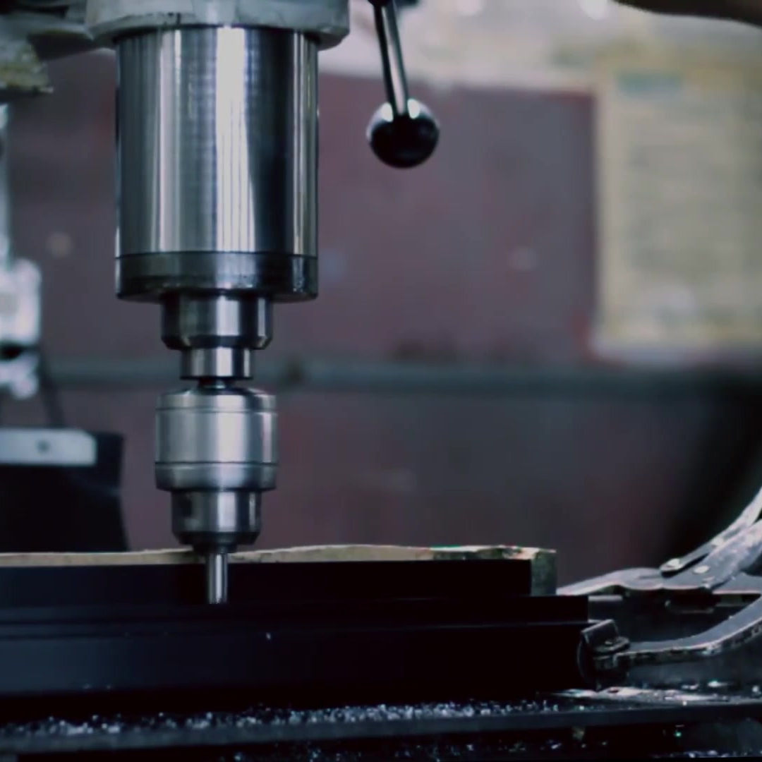
Microscale Manufacturing / Micromanufacturing / Micromachining / MEMS


MICROMANUFACTURING, MICROSCALE MANUFACTURING, MICROFABRICATION or MICROMACHINING refers to our processes suitable for making tiny devices and products in the micron or microns of dimensions. Sometimes the overall dimensions of a micromanufactured product may be larger, but we still use this term to refer to the principles and processes that are involved. We use the micromanufacturing approach to make the following types of devices:
Microelectronic Devices: Typical examples are semiconductor chips that function based on electrical & electronic principles.
Micromechanical Devices: These are products that are purely mechanical in nature such as very small gears and hinges.
Microelectromechanical Devices: We use micromanufacturing techniques to combine mechanical, electrical and electronic elements at very small length scales. Most of our sensors are in this category.
Microelectromechanical Systems (MEMS): These microelectromechanical devices also incorporate an integrated electrical system in one product. Our popular commercial products in this category are MEMS accelerometers, air-bag sensors and digital micromirror devices.
Depending on the product to be fabricated, we deploy one of the following major micromanufacturing methods:
BULK MICROMACHINING: This is a relatively older method which uses orientation-dependent etches on single-crystal silicon. The bulk micromachining approach is based on etching down into a surface, and stopping on certain crystal faces, doped regions, and etchable films to form the required structure. Typical products we are capable of micromanufacturing using bulk micromachining technique are:
- Tiny cantilevers
- V-groves in silicon for alignment and fixation of optical fibers.
SURFACE MICROMACHINING: Unfortunately bulk micromachining is restricted to single-crystal materials, since polycrystalline materials will not machine at different rates in different directions using wet etchants. Therefore surface micromachining stands out as an alternative to bulk micromachining. A spacer or sacrificial layer such as phosphosilicate glass is deposited using CVD process onto a silicon substrate. Generally speaking, structural thin film layers of polysilicon, metal, metal alloys, dielectrics are deposited onto the spacer layer. Using dry etching techniques, the structural thin film layers are patterned and wet etching is used to remove the sacrificial layer, thereby resulting in free-standing structures such as cantilevers. Also possible is using combinations of bulk and surface micromachining techniques for turning some designs into products. Typical products suitable for micromanufacturing using a combination of the above two techniques:
- Submilimetric size microlamps (in the order of 0.1 mm size)
- Pressure sensors
- Micropumps
- Micromotors
- Actuators
- Micro-fluid-flow devices
Sometimes, in order to obtain high vertical structures, micromanufacturing is performed on large flat structures horizontally and then the structures are rotated or folded into an upright position using techniques such as centrifuging or microassembly with probes. Yet very tall structures can be obtained in single crystal silicon using silicon fusion bonding and deep reactive ion etching. Deep Reactive Ion Etching (DRIE) micromanufacturing process is carried out on two separate wafers, then aligned and fusion bonded to produce very tall structures that would otherwise be impossible.
LIGA MICROMANUFACTURING PROCESSES: The LIGA process combines X-ray lithography, electrodeposition, molding and generally involves the following steps:
1. A few hundreds of microns thick polymethylmetacrylate (PMMA) resist layer is deposited onto the primary substrate.
2. The PMMA is developed using collimated X-rays.
3. Metal is electrodeposited onto the primary substrate.
4. PMMA is stripped and a freestanding metal structure remains.
5. We use the remaining metal structure as a mould and perform injection molding of plastics.
If you analyze the basic five steps above, using the LIGA micromanufacturing / micromachining techniques we can obtain:
- Freestanding metal structures
- Injection molded plastic structures
- Using injection molded structure as a blank we can investment cast metal parts or slip-cast ceramic parts.
The LIGA micromanufacturing / micromachining processes are time consuming and expensive. However LIGA micromachining produces these submicron precision molds which can be used to replicate the desired structures with distinct advantages. LIGA micromanufacturing can be used for example to fabricate very strong miniature magnets from rare-earth powders. The rare-earth powders are mixed with an epoxy binder and pressed to the PMMA mold, cured under high pressure, magnetized under strong magnetic fields and finally the PMMA is dissolved leaving behind the tiny strong rare-earth magnets which are one of the wonders of micromanufacturing / micromachining. We are also capable to develop multilevel MEMS micromanufacturing / micromachining techniques through wafer-scale diffusion bonding. Basically we can have overhanging geometries within MEMS devices, using a batch diffusion bonding and release procedure. For example we prepare two PMMA patterned and electroformed layers with the PMMA subsequently released. Next, the wafers are aligned face to face with guide pins and press fit together in a hot press. The sacrificial layer on one of the substrates is etched away which results in one of the layers bonded to the other. Other non-LIGA based micromanufacturing techniques are also available to us for the fabrication of various complex multilayer structures.
SOLID FREEFORM MICROFABRICATION PROCESSES: Additive micromanufacturing is used for rapid prototyping. Complex 3D structures can be obtained by this micromachining method and no material removal takes place. Microstereolithography process uses liquid thermosetting polymers, photoinitiator and a highly focused laser source to a diameter as small as 1 micron and layer thicknesses of about 10 microns. This micromanufacturing technique is however limited to production of nonconducting polymer structures. Another micromanufacturing method, namely “instant masking” or also known as “electrochemical fabrication” or EFAB involves the production of an elastomeric mask using photolithography. The mask is then pressed against the substrate in an electrodeposition bath so that the elastomer conforms to substrate and excludes plating solution in contact areas. Areas that are not masked are electrodeposited as the mirror image of the mask. Using a sacrificial filler, complex 3D shapes are microfabricated. This “instant masking” micromanufacturing / micromachining method makes it also possible to produce overhangs, arches…etc.